

A designer uses electronic components for building up the circuit so that it functions properly. Rush PCB recommends dividing the entire exercise into three distinct activities:
- Component Selection
- Component Sourcing
- Component Placement
A mistake in one or more of the above steps can cause major project complications. It can even lead to non-functioning products, causing delays and holds in a company’s time-to-market.
Component Selection
When a designer conceives a circuit, they usually base it on one or more active components. In most cases, the functioning of an active component depends on the value and rating of a few passive components. Although the designer may have calculated and selected a proper value for the passive component, they commonly overlook other parameters such as:
Power Rating: Designers commonly miss power ratings for resistors. Selecting the power rating of a resistor depends on the maximum current passing through it. CAD libraries often use a standard rating when the designer calls for a component from its library. Not replacing it with a proper power rating can result in a burnt resistor and a non-functioning board.
Voltage Rating: Selecting a capacitor requires the designer to specify its capacitance value, its temperature characteristics, and its voltage rating. While the capacitance value and temperature characteristics directly affects the circuit functioning, specifying the voltage rating depends on the operating voltage of the circuit. Specifying a higher voltage rating than necessary may result in a bulkier package, while under-specifying the voltage rating may result in the capacitor blowing up.
Current Rating: Although the inductance value is the governing factor when specifying an inductor, overlooking the maximum current flowing through the inductor may cause it to operate at a higher temperature or even melt during operation.
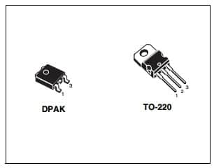
Footprint Pattern: Contrary to popular belief, designers getting footprint patterns wrong is very common not only for passive components, but also for active components. Component manufacturers offer different packages of the same component, to help in design and assembly. PCB CAD libraries also have multiple footprint patterns matching the various packages from the manufacturers. Manufacturers identify different packages for the same component with unique type numbers.
The designer must select the proper footprint from the library, matching the chosen package, and the calculated power, voltage, and current rating of the component. For instance, an active power device may have different footprints based on the manner of its mounting on the PCB for thermal management—the designer must decide beforehand whether the power component will use a separate heat sink or use the copper pattern for effective removal of heat—as the two packages will differ substantially.
Part Obsolescence: While making a selection, the designer must also check if the component will be available from the manufacturer for some time, and they have not listed it for obsolescence soon. Depending on the application, the product and components may have to be available not only for the planned lifetime of the product, but also for some years beyond that time.
The above selection criterion for components is very important as the design is still in the early stages, where changes do not take much time and their cost effect is low. Whatever component the designer decides to use, its unique type number goes into the Bill of Materials (BOM), and carries forward to the following stages.
Rush PCB recommends a session of Design for Manufacturing (DFM) and Design for Assembly (DFA) before the designer finalizes the schematic, and releases the BOM and Gerber files for component procurement and PCB fabrication.
Read About: HOW TO MAKE PCBS MORE RELIABLE?
Component Sourcing
This stage can have more pitfalls than one can normally conceive. One of the most common problems OEMs face is component shortage. For several reasons, many electronic components are in limited supply, with brokers and dealers making available expected products weeks or even months after the promised date.
Limited Supply: High demand and limited supply have additional consequences, such as higher prices and project delays. Often, locating hard-to-find components leads to new minimum order quantities, forcing buyers to purchase more than necessary at higher prices.
Alternative Sources: The inability to source a specific component in the BOM within a reasonable time limit may require the designer to look for alternatives. Although this is a regular practice with designers, it is more common for them to specify alternatives for active components alone. However, circumstances are adding passive components as well to the shortages list.
Counterfeit Components: Component shortages are leading to another negative impact such as counterfeits. Scrupulous agents are relabeling defective, wrong, and/or out-of-date parts and feeding them into the supply chain. OEMs without stringent sourcing arrangements may inadvertently use these sub-standard components resulting in problems of product functionality.
Rush PCB offers full-turnkey assembly services, so our customers do not face problems of component sourcing. We maintain special relationship with component manufacturers and top-tier component suppliers, and work directly with them for securing the necessary components in time. We also hold an in-house inventory of high-demand parts to meet customer requirements for the next 12 months.
However, we are always open to substitutions and customers supplying their own parts and boards for assembly. For small components such as 0201, 0402, and 0603, we may ask for additional quantity to account for losses during assembly.
Component Placement
For achieving a reliable and repeatable placement process, designers must consider the following points:
- Gerber Data
- Panel Size
- Handling Strips
- Fiducial Marks
- Component Size and Position
- Component Supply
Gerber Data: this information provides the pick and place machines information on component position and rotation. Unless this data is accurate and unambiguous, the resulting output can be disastrous. CAD generated data is usually accurate, however, with PCB designs usually undergoing changes, designers must be careful in sending the relevant data set to the fabricator.
Read About: DEBUGGING A NON-WORKING PCB
Panel Size: for increasing the efficiency of the fabrication and assembly process, fabricators group PCBs into panels. Each machine has its specified maximum and minimum board size it can process. The designer must have knowledge of the board size the fabricator’s machine can process effectively and add suitable fabricating instructions.
Handling Strips: for proper handling of panels during fabrication and assembly, panels require handling strips along at least two of their opposite sides. Designers must include the handling strips in their design, taking care to avoid positioning components inside the area of the handling strips, and within a certain distance from the edge.
Fiducial Marks: these allow accurate positioning of components by pick and place machines, especially for fine-pitch components. The machines use their vision systems to locate these unique marks on the track layer of the PCB/panel and align themselves.
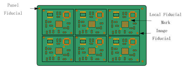
Rush PCB advises designers to place two fiducial marks at diagonally opposite corners on the PCB, and this is adequate for placement of larger components. For components requiring greater accuracy, designers must place additional fiducial marks near the component.
Component Size and Position: in densely populated boards designers often place small components close to larger components. This may require the placement program generator to place the smaller components before the machine can place larger parts, without causing any disturbance. It is also necessary for the designer to place the parts ensuring they have adequate gaps in between, to allow the machine place all components without disturbance.
Component Supply: Manufacturers supply surface mount components in several ways, most common being tape, reel, tubes, and trays. Machines usually have feeders capable of handling all types of packaging in larger quantities, and there can be problems when assembling only small quantities of components for a small batch of PCB assembly, especially when the components are available in cut tapes. Assemblers may have to manually place the components, repackage them suitably so that the machines accept them, or use special attachments for using the cut tapes.
Conclusion
Although component selection and placement are a relatively straight forward concept for PCB assembly, there can be many pitfalls causing confusion, delays, and cost escalations during assembly. Our customers can avoid all the above problems by taking advantage of our offer of free DFA and DFM exercises before production runs, and the full-turnkey service from Rush PCB for fabrication and assembly of their projects.


