

According to the assembly and testing experience gathered by Rush PCB, there can be several reasons why the newly assembled PCB fails to function as intended during testing. We list below the most likely broad causes for a non-working PCB. However, each of them may be due to several independent issues.

- Bad Component
- Wrong Design Assumptions
- Overheating
- Bad Power Supply
- Noise in the Circuit or near it
- Wrong Connection
- Bad or No Connection
Bad Component
A bad electronic component will not allow the circuit to function as intended either completely or partially, depending on its position in the schematic. For instance, if the component in question is in series with the power supply lines, it may prevent power from reaching the rest of the circuit. Reasons for the component being bad may be many, but some of them could be:
The component was faulty on receipt: this can be a quality issue with the supplier, a packing problem during transportation, or a handling problem at the receipt counter.
The component went bad during storage: this can be due to problems during storage, such as caused by ESD.
The component went bad during assembly: most likely cause is bad handling leading to mechanical damage, or failure to adhere to ESD requirements.
The component went bad after assembly: we discuss the reasons for this as below.
Wrong Design Assumptions
It is possible for a component to go bad after assembly and during testing, when the operator fed power to the circuit. Although the primary reason for this would be a wrong design assumption by the designer, it can also be due to other reasons such as:
Wrong component: it is possible that component ratings do not match the specifications, designer has underspecified the component ratings for the circuit, or the component has failed because of a wrong design assumption for some other component. For instance, a low resistance value can lead to the failure of an LED.
Overheating
A surge of current can lead to an increase in the temperature of a component. Depending on whether the current build-up is gradual or sudden, the temperature of the component may rise slowly or exponentially, until the circuit starts to malfunction or stops functioning altogether. Almost all the reasons stated above can lead to overheating.
Bad Power Supply
While testing, an operator may have to connect a power supply to the assembled PCB. If the power supply is out of calibration, the protection circuits are non-functional, or the power supply has undetected internal problems, it can damage the circuit to which the operator connects it.
The circuit under test may have internal power supplies delivering different voltages to various sections of the circuit. If any these power supply modules are not functioning properly, the circuits they supply will also not perform as intended.
Read About: MANUFACTURING PCBS FOR INDUSTRIAL BUSINESSES
Noise in the Circuit or near it
It is possible noise in the circuit or near it is preventing the circuit under test from functioning as intended. This may be because of several reasons, starting from bad component, wrong EMI/EMC design assumptions, to a bad power supply.
If a nearby device is coupling noise into the circuit under test, and causing it to malfunction, the operator may have to switch off the device during the period of the test. As the situation is one of electromagnetic compatibility, Rush PCB recommends notifying the designer about the problem.
Wrong Connection
A wrong connection can lead to a circuit under test from performing up to expectations and even stop functioning altogether, depending on how it affects the circuit. Moreover, a wrong connection may be the result of a wrong design assumption or one due to bad execution during assembly—a wrong wire connection, for example.
There can be many instances of wrong design assumptions leading to a wrong connection. A wrong footprint for an active component being the most common example.
A wrong connection in the schematic may carry over to the layout and ultimately appear in the fabricated PCB as a wrong track. This is one of the most difficult things to debug in a non-working PCB, and is an expensive mistake, as it becomes necessary to scrap the entire fabrication exercise.
During the etching process, a sliver of copper may detach and lodge itself at another location on the board causing a wrong connection. However, this is an isolated incident and may cause only one or a few boards to stop functioning.
During the solder paste printing process, excess solder deposit near fine pitch components may result in solder bridging during reflow. Solder bridging also causes electrical connections at places where they should not be existing, leading to non-functional PCBs.
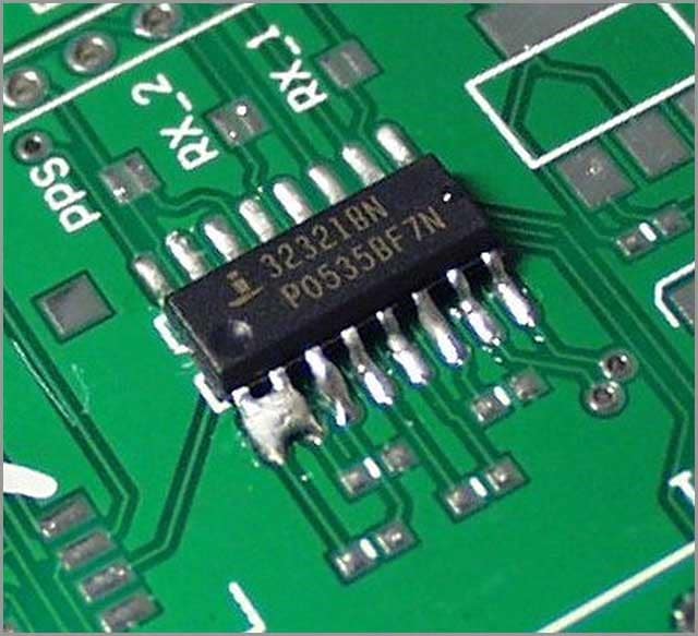
Wave soldering often causes through-hole components to tilt, especially if the design has low lead-to-hole diameter ratios. Neighboring leads can tilt towards each other and form a solder bridge under the board, causing a wrong connection.
Read About: WHAT IS FULL TURNKEY PCB SERVICE?
Bad or No Connection
An electric circuit functions properly and as intended only when all interconnections are in place. Any wrong connection, bad, or no connection will alter the functioning of the circuit in different ways depending on the nature of the wrong connection. There can be several reasons for a bad or no connection in a circuit board assembly.
Bad or no-connection in a bare PCB: The designer may have caused this by a wrong design assumption, a bad photo-lithography process—presence of dirt below film may have caused it, or it may have been due to over-etching in the acid bath.
Mismanagement of change is a very common reasons for wrong, bad, or no connections in a PCB. Designs undergo iterations before sending the documents over to the fabricator. In many cases, iterations take place even as the fabricator is working with one set of design documents, while designers are busy adding or deleting functions to the PCB.
Unless the designer manages the changes above properly, the fabricator may end up with an older set of documents that are marginally different from those for the final PCB. Such miscommunications between the OEM and the fabricating house are quite common and result in delays, extra expense, and lengthening of the time-to-market.
Conclusion
Rush PCB recommends two processes to take care of the issues above—Design for Manufacturing (DFM) and Design for Assembly (DFA). Diligently following the two processes can weed out most of the problems leading to a non-working PCB, so that the occasion for debugging one does not arise. By following DFM and DFA procedures, the PCB turns out right first time in nearly 99% of cases.


