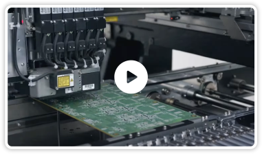
PCB Assembly Rework Services in the USA
PCB assembly rework involves removing, replacing or modifying components on a populated printed circuit board (PCB) to bring the assembly into compliance with applicable requirements. The challenge is to correct the original defect or implement the required modification without damaging the PCB, surrounding components or underlying interconnections.
RUSH PCB has provided PCB assembly rework services since 2004, supporting a wide range of applications, including 0201 chip passives, 0.3 mm-pitch BGAs, 30-layer backplanes, rigid-flex assemblies and boards requiring component-level modifications.
Whether a production line has stopped, a completed assembly has failed first article inspection, an engineering change order (ECO) affects boards that have already been built, or field-return assemblies need to be evaluated for rework, our team can help determine the appropriate approach.
Most rework lots are completed within 3–7 business days, with expedited turnaround of 24–48 hours available for qualifying urgent projects, subject to complexity, parts availability and workload.
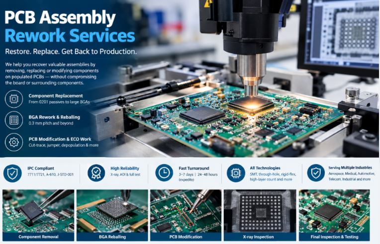
Call 1-408-496-6013 or email [email protected] to request a PCB rework quote.
A populated PCB assembly can contain hundreds or thousands of dollars in components, with some assemblies representing significant material and manufacturing costs. Scrapping a defective assembly can mean losing that investment while also creating additional replacement costs and potentially long component lead times.
PCB rework can help recover that value by correcting identified defects, replacing components or implementing approved engineering changes without manufacturing an entirely new assembly.
Common PCB assembly rework requirements include:
- Engineering change orders (ECOs) affecting completed assemblies
- Incorrect, damaged or suspect component replacement
- Solder bridging and other soldering defects
- Excessive voiding and head-in-pillow defects
- Component-related ICT and functional test failures
- Obsolete or discontinued component replacement
- Field-return assembly evaluation
- Lifted pad and damaged trace correction where applicable to the approved rework process
- Plated-through-hole and via-related work where supported by the required procedure
- Prototype modifications and engineering changes
- Cut-trace and jumper-wire modifications
- Component depopulation and recovery
Each PCB assembly should be evaluated individually to determine the appropriate rework procedure, acceptance criteria and verification requirements.
Types of PCB Rework Services
Component Removal and Replacement
Component-level PCB rework can include:
- BGA, micro-BGA (µBGA) and CSP devices, including pitches down to 0.3 mm, subject to package dimensions and board design
- QFN, LGA and DFN packages, including bottom-terminated components with thermal pads
- QFP, TQFP, SOIC, SOP and other leaded SMT packages
- 0201 metric chip passives and larger components
- Tombstoned component correction
- Through-hole components
- Multi-pin headers and press-fit connectors
- High-thermal-mass ground pins
- Package-on-package (PoP) separation and reassembly
- RF shields, heat sinks, stiffeners and standoffs
The feasibility of each operation depends on the component package, PCB construction, pad geometry, thermal limitations and accessibility of the rework site.
BGA Rework and Reballing
BGA rework requires controlled thermal processing, accurate component alignment and careful preparation of the PCB land pattern.
The process can include:
- Controlled BGA removal
- Solder site preparation
- Inspection of the PCB land pattern
- BGA reballing where component reuse is appropriate
- Accurate component placement
- Controlled reflow
- Post-rework inspection and testing
Rework equipment can use closed-loop temperature control, thermocouple-based profiling, bottom-side preheating and vision-assisted placement.
Where a BGA is suitable for reuse, residual solder can be removed and the package prepared for reballing. New solder spheres are applied using the specified alloy and diameter, followed by inspection before the component is reinstalled.
Both lead-free and tin-lead soldering processes may be supported where permitted by component requirements, customer specifications and applicable regulations.
X-ray inspection can be used to evaluate hidden solder joints before and after BGA rework where appropriate to the assembly and inspection requirements.
PCB Modification and ECO Work
PCB assembly rework may also be required when an engineering change must be implemented on assemblies that have already been manufactured.
Modification work can include:
- Cut-trace modifications
- Jumper-wire installation
- Component substitutions
- Component removal
- Component additions
- Wire modifications
- ECO implementation
- Conformal coating removal at the rework location
- Conformal coating reapplication where required
- Underfill and staking material removal and reapplication where appropriate
- Depopulation of specified components
- Component harvesting
- Lead-free and tin-lead processing where applicable
Modification requirements should be supported by approved engineering documentation and clear acceptance criteria before work begins.
PCB Assembly Rework Process
A controlled PCB rework process helps reduce the risk of additional damage while providing a documented basis for evaluating the completed assembly.
1. Assembly Evaluation and Fault Identification
The assembly is reviewed against the supplied rework instructions, ECO documentation, drawings and applicable specifications.
If the fault has not already been identified, suitable diagnostic methods may include:
- X-ray inspection
- Automated optical inspection (AOI)
- Electrical probing
- Continuity testing
- In-circuit testing (ICT)
- Functional testing
The objective is to identify the likely cause of failure, determine the affected components or interconnections and establish whether PCB rework is technically feasible.
2. Rework Planning and Thermal Profiling
A rework plan is developed according to the assembly requirements and applicable IPC-7711/7721 procedures.
Thermal profiling can use representative test assemblies, suitable process-development samples or other validated methods. Thermocouples may be used to measure temperatures at critical locations and verify that the process remains within relevant component and PCB limits.
The thermal profile should account for the most temperature-sensitive components and materials on the assembly, not only the component being removed or replaced.
3. Controlled Preheating
Appropriate preheating helps reduce temperature gradients across the PCB and minimise thermal stress during localised heating.
The preheat conditions must be suitable for the laminate, component packages, moisture sensitivity and selected soldering process.
Poorly controlled heating can contribute to thermal shock, pad damage, laminate delamination and damage to nearby components.
4. Component Removal
Once the assembly reaches the required temperature conditions, localised heating is applied to bring the relevant solder joints to the appropriate reflow temperature.
The component is then removed using suitable equipment and handling methods designed to minimise mechanical stress on the PCB pads and surrounding structure.
5. Solder Site Preparation
Residual solder is removed using appropriate methods, and the exposed land pattern is inspected under suitable magnification.
The area is checked for:
- Lifted pads
- Damaged solder mask
- Contamination
- Damaged lands
- Other PCB defects that could affect the rework
Any condition identified should be assessed before the replacement component is installed.
6. BGA Reballing
When a BGA is suitable for reuse, the existing solder is removed and the ball-attachment surfaces are prepared.
New solder spheres of the specified size and alloy are applied using a controlled process. The reballed component is inspected for relevant defects, including ball placement and coplanarity, before reinstallation.
7. Component Placement and Reflow
The replacement or prepared component is aligned with the PCB land pattern using suitable placement equipment.
The assembly is then heated according to the validated thermal profile to establish the required solder joints.
The process must account for:
- Component temperature limits
- PCB thermal mass
- Solder alloy
- Pad geometry
- Nearby components
- PCB construction
8. Inspection and Testing
After PCB rework, the assembly is inspected and tested according to the applicable product requirements and agreed acceptance criteria. For additional information on PCB assembly reliability, see the linked page.
Verification may include:
- Visual inspection
- High-magnification inspection
- X-ray inspection
- AOI
- Continuity testing
- ICT
- Functional testing
- Ionic contamination testing
- Cross-section analysis
- Dye-and-pry analysis where appropriate
Inspection methods are selected according to the assembly, defect type and required level of verification.
9. Rework Documentation
Completed assemblies can be accompanied by agreed rework documentation, including:
- Rework reports
- Inspection records
- Relevant X-ray images
- Test results
- Traceability information
Documentation requirements should be established before work begins, particularly for aerospace, defence, medical and other high-reliability applications.
PCB Rework Standards and Quality Requirements
PCB assembly rework should be controlled according to applicable industry standards, customer specifications and product requirements.
Relevant standards may include:
- IPC-7711/7721: Procedures for electronic assembly rework, modification and repair
- IPC-A-610: Acceptability of electronic assemblies
- IPC J-STD-001: Requirements for soldered electrical and electronic assemblies
- IPC/JEDEC J-STD-033: Handling and use of moisture/reflow-sensitive devices
- ISO 9001: Quality management system requirements, where applicable
- RoHS and REACH: Applicable substance and chemical compliance requirements
- ANSI/ESD S20.20: Electrostatic discharge control requirements, where applicable
The exact standards and acceptance criteria depend on the product, application, customer requirements and contractual specifications.
PCB Assembly Rework for Different Industries
PCB assembly rework can support manufacturers and engineering teams across a range of industries.
Military and Aerospace PCB Rework
Military and aerospace electronics can require Class 3 acceptance criteria, detailed traceability, specialised inspection and controlled soldering processes.
Medical Electronics Rework
Medical electronics may require controlled rework procedures, cleanliness verification, traceability and documented inspection and testing depending on the device and applicable quality requirements.
Automotive and EV Electronics
Automotive and electric vehicle electronics can be exposed to thermal cycling, vibration and demanding operating conditions. PCB rework must account for the assembly’s reliability requirements and applicable customer specifications.
Telecom and Networking PCB Rework
Telecommunications equipment often uses complex assemblies, large BGAs and high-layer-count backplanes. PCB rework must consider board construction, thermal mass, interconnect design and nearby components.
Industrial Electronics and Semiconductor Equipment
Industrial and semiconductor equipment may depend on specialised or obsolete PCB assemblies. Rework can help extend equipment service life where replacement assemblies or components are difficult to obtain.
Consumer Electronics and IoT
Component replacement, engineering modifications and depopulation can support prototype development, product updates and selected component recovery projects.
Research and Development
Engineering teams, research laboratories and university facilities may require prototype modifications, jumper installation, component replacement and other PCB modifications for design validation and troubleshooting.
Why Choose RUSH PCB for PCB Assembly Rework?
PCB Fabrication and Assembly Experience
Understanding PCB construction is important when planning component-level rework. Stack-up, copper distribution, laminate properties, via structures and thermal mass can influence the rework process.
Engineering-Led Rework Assessment
PCB rework is more than simply removing a component and installing another one. Effective rework begins with understanding the failure, evaluating the condition of the PCB and selecting an appropriate process.
Controlled Thermal Processing
Thermal profiling and controlled heating are important when working with complex PCB assemblies. The process must consider component temperature limits, PCB construction and surrounding components.
Inspection and Verification
Hidden solder joints and internal PCB structures may require inspection methods beyond visual examination. X-ray, AOI and electrical testing can provide additional information when appropriate for the assembly and defect.
Experience With Complex PCB Constructions
High-layer-count boards, HDI assemblies, laser-drilled microvias, blind and buried vias, flexible PCBs, rigid-flex assemblies and specialised laminates can present different thermal and mechanical challenges during rework.
Prototype and Production Quantities
PCB rework requirements can range from a single prototype modification or field-return assembly to larger production rework and component recovery projects.
What to Include With a PCB Rework Request
Providing complete information helps establish the scope, feasibility, cost and expected turnaround time.
Where available, include:
- Assembly quantity – Number of PCBs requiring rework and number of rework locations per assembly.
- Component details – Reference designators, package types and affected component part numbers.
- Technical drawings – Assembly drawings, fabrication drawings, stack-up details and relevant Gerber or ODB++ files.
- Bill of materials – BOM and replacement component part numbers.
- ECO or rework instructions – Approved engineering change orders or work instructions.
- Acceptance requirements – Required IPC-A-610 class and additional customer requirements.
- Replacement components – Confirmation of whether components are customer-supplied or need to be sourced.
- Turnaround requirements – Required completion date and whether expedited processing is needed.
- Soldering requirements – Lead-free or tin-lead requirements and applicable restrictions.
- Known defects and test results – Failure descriptions, photographs, X-ray images and electrical or functional test results.
If complete documentation is unavailable, photographs, component markings, board details and a description of the problem can provide a starting point for assessment.
Frequently Asked Questions About PCB Assembly Rework
What Is PCB Assembly Rework?
PCB assembly rework is the controlled process of removing, replacing or modifying components on an already assembled PCB.
It may be required to correct manufacturing defects, replace incorrect or obsolete components, implement an engineering change or address an assembly identified during testing or inspection.
What Is the Difference Between PCB Rework and PCB Modification?
PCB rework generally involves correcting a non-conforming assembly or replacing components to meet the applicable requirements.
PCB modification involves making an approved design change to an existing assembly. Examples include component substitutions, jumper wires, cut traces and other ECO-related changes.
The two processes can overlap depending on the project requirements.
How Many Times Can a PCB Be Reworked?
There is no universal rework-cycle limit that applies to every PCB, component and product.
The acceptable number of rework cycles depends on PCB construction, component limitations, applicable specifications, customer requirements and the thermal history of the assembly.
Repeated thermal exposure can increase the risk of laminate, pad, interconnect and component damage.
Can a BGA Be Removed and Reused?
In many cases, a BGA can be removed, reballed and reinstalled if the component remains suitable for reuse.
The BGA should be inspected for conditions such as cracking, delamination and moisture-related damage before reuse.
Can a Reworked Solder Joint Meet the Same Acceptance Criteria?
A reworked solder joint can meet the applicable workmanship acceptance criteria when the process is properly controlled and verified.
Long-term reliability depends on factors including thermal history, PCB and component condition, solder alloy compatibility, process control and the operating environment.
Can You Rework PCBs From Another Manufacturer?
Yes. PCB rework can be performed on assemblies manufactured or assembled by another supplier, subject to technical assessment.
PCB construction, documentation, component condition and the nature of the required rework determine the feasibility and scope of the work.
What Is the Minimum PCB Rework Quantity?
A single assembly may be suitable for rework depending on the technical requirements and scope of the project. Larger production lots can also be evaluated.
How Fast Can PCB Rework Be Completed?
Standard rework lots typically require 3–7 business days, depending on complexity, parts availability, documentation and testing requirements.
Expedited 24–48-hour turnaround may be available for qualifying urgent projects.
Can Lead-Free Assemblies Be Converted to Tin-Lead?
Conversion may be possible depending on the assembly, component specifications, soldering requirements and applicable regulations.
The required process and materials should be established before work begins.
Can Conformal Coating Be Removed and Reapplied?
Selective conformal coating removal and reapplication may be possible depending on the coating type, PCB materials, components and rework location.
How Are Moisture-Sensitive Devices Handled During PCB Rework?
Moisture-sensitive devices should be handled according to applicable requirements, including IPC/JEDEC J-STD-033 where specified.
Depending on the device classification and exposure history, controls can include moisture-barrier storage, floor-life monitoring and baking under approved conditions.
Request a PCB Assembly Rework Quote
Need to replace a BGA, correct a soldering defect, replace a component or implement an engineering change?
Send your PCB assemblies, component details and available technical documentation for assessment.
RUSH PCB can evaluate the technical requirements, determine an appropriate rework approach and identify the inspection and testing requirements for your project.
Whether you need a single prototype modification, a small production lot or a larger assembly rework programme, the required process can be assessed based on your PCB construction, components and acceptance criteria.
Call 1-408-496-6013 or email [email protected] to request a PCB assembly rework quote.