

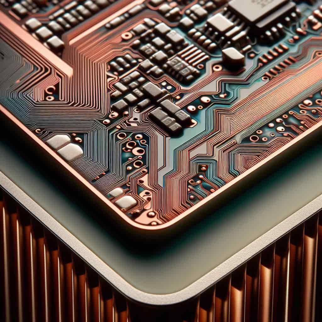
Rush PCB Inc. makes various types of high-quality PCBs or Printed Circuit Boards for the electronic industry. While each PCB can have an individual and unique boundary or perimeter, it typically defines the extent of the electronics mounted on that PCB. Apart from that, the perimeter can also serve other functions.
The most notable function of the perimeter of a printed circuit board is its definition of a routable area. Each layer in the stack-up has a positional variation, and the designer must compensate for this by reserving a small area from the edge, where metal must not intrude.
Most fabricators prefer to pull back the metal from the edge by about 0.2 mm (8 mils). However, many can go up to 0.125 mm (5 mils), while others, defining the PCB edge with lasers, allow the metal to be within 0.05 mm (2 mils) of the edge.
What is Edge Plating?
Some PCBs require edge plating—allowing the metal right up to the edge and wrap the plating around to the other side. This is edge plating, and designers use it for creating a complete Faraday cage around a circuit, thereby preventing EMI or Electromagnetic Interference from leaking to the outside of the board and disturbing neighboring circuits. If necessary, designers can use the edge plating to pass ground and or power from the top to the bottom around the edge of the board. In some cases, designers prefer to use a slot within the outline of the board for passing ground and power, rather than the edge plating.
Designers inform PCB fabricators of their intentions by drawing the shapes right up to the edge on both sides and specifying that these locations must have metal wrapping around them. This is not an isolated requirement, as many users ask for edge plating. Apart from preventing EMI emissions from leaving the board, edge plating has the added advantage of preventing the inner layers from absorbing moisture through the board edges. However, edge plating has other uses as well.
Edge Plating and Gold Fingers
Rather than mounting a connector on the edge of the board, it is possible to use the board itself as a part of a connector. Edge plating in the form of a row of gold fingers can act as a connector, with the gold fingers being plated on both sides of the board edge. Of course, the designer must ensure the PCB has a standard thickness of 1.6 mm (0.062 inches), for the fingers on both sides to properly engage with the receptacle.
For instance, computer motherboards often have PCIE connectors as a common interface, making use of gold fingers on a board’s edge. The board forms one-half of the connector pair. Designers typically pull back a few of the gold fingers to allow these connections to be made later and disconnect first.
Another example of edge plating on a board being used as a connector is by flex circuits. These are typically useful as bespoke cables connecting two rigid boards. Flex circuits typically use a ZIF or Zero-Insertion-Force connector as an expansion of the finger idea. The ZIF connector has an additional row of contacts that fit into a companion connector with a latch to lock the tail of the ZIF once the user inserts it.
A designer can easily create the PCIE connector footprint in their libraries. However, the ZIF connector footprints are more complicated as they must mate with the companion connector. Most connector vendors, therefore, usually provide the interlocking footprint in popular ECAD formats.
Edge Plating for HDMI
HDMI or High-Definition Multimedia Interface also uses edge connectors. Although their design has a simpler geometry, their specification requires more durable gold on the edges to cater to the necessary 10-thousand insertion and extraction cycles without failure. This requires fabricators to use hard gold as a selective plating step only for the edge connector.
HDMI gold fingers require the gold plating to extend to the very edge of the board. As the cost of this plating step is high, most fabricators prefer to forego it if the designer wants it as an absolute necessity. On the other hand, the specification for a USB dongle is it must survive at least 5-thousand cycles of insertion and extraction.
Edge Plating for USB
The USB implementation of edge connectors uses a low-headroom environment. Laptops, tablets, and smartphones typically have a mid-mount connector for USB. Usually, this is a cut-out in the board’s edge where the connector body sits. Most connector vendors prefer to have tight tolerances that describe a cut-out feature with a minimum and or a maximum value.
The Edge Plating Process
Fabricators face several challenges during the edge plating of boards, one of them being precision handling. They must prepare the edges properly for the plating process, which must create a lifetime adhesion of the plated material. The fabricator must use a controlled process while fabricating the board to limit any potential hazard for the edge plating. Their chief concern is the creation of burrs, which often leads to discontinuities in PTH walls and reduces the adhesion of the edge plating.
While edge plating on PCBs is a simple addition, fabricators need trained personnel and specialized equipment for the process. Designers must ensure to not allow internal power planes to come right up to the edge, while fabricators must make sure of a gap being present before they take up edge plating. Moreover, designers must ensure the presence of a band of copper on both edges on the top and bottom sides of the board, as the plating will connect these bands.
As fabricators will be holding the board within production panels during the processing, plating around the complete length of the edge will not be possible. There will be some gaps where they will place route tabs. For manufacturing a board with edge plating, the fabricator must route the board profile at the place of the edge plating before starting the process of through-hole plating. Therefore, there cannot be V-cut scoring on boards that undergo edge plating.
Successful edge plating requires designers to confirm beforehand with their fabricators the extent to which the fabricator can edge plate the board. They must indicate the need for edge plating clearly on a mechanical layer, and the surface finish they need on it. Fabricators typically favor a selective chemical nickel-gold as a surface finish on a round edge plating.
Edge Plating Applications
Several industries opt for edge-plated boards, especially for applications that require better support for board connections that slide into metal casings. There are other uses of edge plating also, such as it:
● Improves the current-carrying capabilities of the board
● Provides edge connection
● Provides edge protection
● Provides the possibility of edge soldering
● Improves fabrication
Key Process Controls in Edge Plating
Many process controls are necessary during edge plating. For instance, the fabricator must:
● Plating Thickness — necessarily confirm meeting the minimum plating thickness. They can do this by X-ray fluorescence analysis or through microscopic examination.
● Electrical Continuity — verify the electrical connectivity from the inner layers through the plated edge contacts. They must ensure electrical signals can pass through the edge contacts.
● Plating Coverage — inspect the plating for the presence of thin areas or voids around traces. If the plating coverage is inconsistent, it can lead to mechanical or electrical problems.
● Overplating — ensure the plating is not excessively built up on the PCB, as this can lead to interference with the mating of connectors.
● Trace Geometry — confirm that the trace dimensions on the edge contacts match the specifications, as deviations can affect electrical performance.
Conclusion
In the realm of PCB fabrication, the edge plating process is a pivotal technique. According to Rush PCB Inc., this technique is prized in applications demanding tight edge connections, steadfast protection for exposed board edges, and unyielding connectivity. However, this meticulous procedure requires exacting steps to achieve excellent electrical connectivity, mechanical strength, and corrosion resistance.


