

Rush PCB, our customers and most others are accustomed to seeing and handling Integrated Circuits or ICs. However, what everyone sees and handles is really the external packaging, as the die or the chip itself is tiny, fragile, and susceptible to damage by the environment. Moreover, handling the chip itself would be very difficult for the users because of the tight pitch of its connections. Therefore, it is necessary for manufacturers to package the IC chip.
Primarily, the external package helps to spread the connections from the tight pitch on the die to the relatively wide pitch that the user can comfortably handle. Secondly, the package also acts to hermetically seal the chip, that is, enclose it within a sealed compartment so that outside chemicals and gases are unable to reach it. To understand the necessity for the wide variety of IC packages present in the market, it is important to know something about ICs and their functions.
IC Classification
The die of an IC is a conglomeration of interconnected transistors, resistors, capacitors, and diodes to perform specific functions. Once encapsulated in a suitable package, the internal die connects to external components via the terminals present on the package. Manufacturers like to classify different types of ICs based on the size of the die and the number of gates on it:
- SSI — Small Scale Integration, containing 3-30 gates on a single chip.
- MSI — Medium Scale Integration, containing 30-300 gates on a single chip.
- LSI — Large Scale Integration, containing 300-3000 gates on a single chip.
- VLSI — Very Large-Scale Integration, containing more than 3000 gates on a single chip.
Manufacturers also divide ICs based on the techniques they use for manufacturing them. The division follows three broad classes:
Thick and Thin film ICs: Manufacturers integrate the passive components such as resistors and capacitors, leaving out the active components. These thick and thin film ICs are usually a combination of discrete components integrated together.
Monolithic ICs: These are the most common type of ICs available today. A monolithic IC consists of discrete components, both active and passive, and the interconnections between them integrated on a single silicon chip.
Hybrid or Multichip ICs: Mostly used for high power applications, a hybrid or multichip IC may have more than one individual chip interconnected. Manufacturers typically use diffused transistors or capacitors on a single chip for these ICs. They can handle power from 5-50 W.
Users like to differentiate ICs depending on their functionality—Digital Integrated Circuits, Analog Integrated Circuits, and Mixed Signal Integrated Circuits.
IC Packaging
Apart from the manufacturing techniques of classifying ICs listed above, ICs are available in a myriad number of packaging types—the variety is mainly due to evolving technology. For instance, although ICs are available for through-hole mounting, surface mounting types are replacing them fast.
The standard single-in-line (SIP) and dual-in-line (DIP) packages for through-hole mounting does fulfill basic requirements and have been enjoying wide use in the electronic industry for several years. However, with increasing integration, higher speed, and progressive miniaturization of electronic equipment, the industry has been requesting newer packages that will provide:
- Higher number of pins for Input/Output
- Ultra-Miniaturization
- Packages suitable for high-density ICs
- Improved heat resistance suitable for reflow soldering and Lead-free soldering
- Ease of soldering
- Higher throughput speed
- improved heat dissipation
- Lower cost per pin
- Standardization
In response to these requests, IC manufacturers have evolved a diversified family of packages capable of meeting these myriad requirements of the electronics industry.
IC Packages for Through-Hole Mounting
The structure of IC packages for through-hole mounting have lead pins that the user must insert and solder into holes drilled through the printed circuit board (PCB). OEMs use through hole mounting in electronic equipment where board space is not at a premium or where costs are a constraint. Typical packages available are:
SIP or Single In-line Package: This package has the lead pins in a single line and manufacturers use it for transistors and simple ICs.
DIP or Dual In-line Package: These are like SIP, but with two lines of lead pins. The lead pitch is 2.54 mm (100 mil), and the spacing between terminal rows is typically 300, 400, or 600 mil.
IC Packages for Surface Mount Technology (SMT)
Most IC packages for SMT have a flat structure with lead pins soldering directly to the mount pad on the PCB. Useful in applications with high pin density, users can mount these devices on both sides of the PCB.
SOP or Small Outline Package: SOP packages usually have gull-wing leads drawn out of the package body in two opposing directions. With standard lead pitch of 1.27 mm (50 mil), it is possible to mount them flat on the PCB.
SSOP or Shrink Small Outline Package: These are SOPs with lead pitch of less than 1.27 mm.
TSOP or Thin SOP: Ultra-thin SOPs with height of less than 1.27 mm, suitable for ultra-thin equipment such as in smart-cards.
QFP or Quad Flat L-Leaded Package: These packages have gull-wing type leads emanating from all four sides and it is possible to mount the IC flat. QFPs come in large variety of lead pitch even when the dimensions of the package body do not change.
CSP or Chip Size Packaging: Manufacturers use these as mainly packaged wafers which they cut and separate into individual chips.
BGA or Ball Grid Array: These are surface mounting packages with solder ball arrays on their underside surface. Manufacturers offer a large variety of BGA types, some with the solder ball arrays in fine pitch. Some of the more common types are FCBGA, Stacked Chip BGA, and MCMBGA.
Read About: COMPARISON OF THROUGH-HOLE AND SURFACE MOUNT PCBS
More Advanced IC Packages
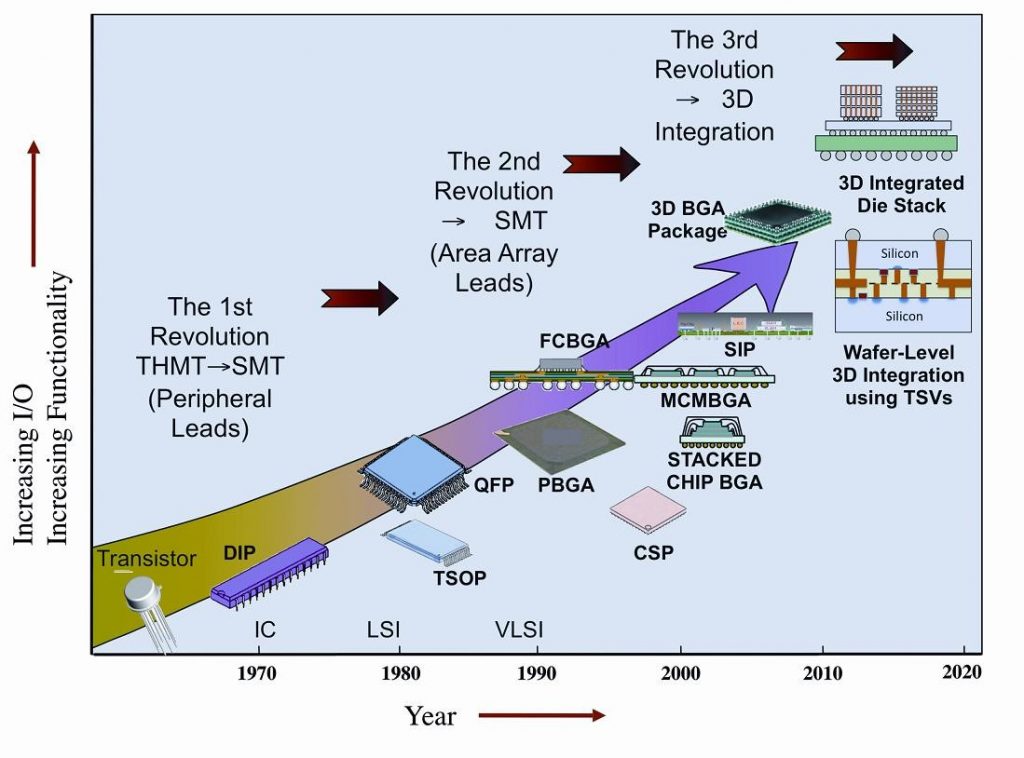
The need to shrink package size and height for miniaturized solutions, simplify the supply chain, and provide a lower overall cost is leading to a drive for Next Level Integration and Wafer Level Packaging (WLP). Manufacturers are shrinking pitches and pads at the chip to package interface much faster than the shrinkage at the package to board interface. This is leading to 3D eWLB package implementation using Through Silicon Via (TSV) applications together with discrete component embedding, resulting in 3D packages such as PBGA, FC-PBGA, 3D BGA, and 3D Integration Die Stack.
Read About: ESSENTIAL STEPS TO KNOW ABOUT BGA
Conclusion
Rush PCB recommends using NSMD or Non-Solder Mask Defined copper landing pads for the most optimum design of BGA boards. As no solder mask covers NSMD pads, they offer the designer maximum flexibility in the breakout for BGA and related packages. We use several advanced fabrication technologies for reducing the number of layers necessary to route designs with advanced IC packages. This helps to balance the increase in fabrication costs of the board.
For PCB design and fabrication with any type of Through-hole, SMT, and other Advanced IC packages, please contact Rush PCB today, over phone or on our website.


