Free PCB Design 2-4 Layers
We will Design your PCB for FREE! Right Here in the Heart of Silicon Valley!
If you are a RUSH PCB 1st Time Customer, we will design your PCB for FREE!
Submit Schematic in *.SCH files, PDF or Hand drawn format to [email protected] or pcb assembly.
- Must be 2 or 4 layers and < 30 square inch
- Please allow 5-7 Days for a complex design
- We will send you the Gerber files and others for you to keep, as long as we are building your board
Rush PCB
Rush PCB is an expert in PCB design for the past 20+ years. For any assigned project, our excellent team works to reduce iterations (revisions), as we simultaneously interact with n-house PCB fabrication, procurement, and assembly teams.
Design engineers at Rush PCB closely interact with R&D and production houses to ensure your product (design) will be delivered in time to market.
Rush PCB’s Experiences & Strengths:
-
- High-Speed PCB Design
- FPGA Design
- HDI Design
- Multi-Layer Design
- Mixed Signal Design
- Blind/Buried Via Design
- TDR Traces
- Length-Matched Traces
- Fine Pitch BGA
- Constraint Manager
- DFM
- DFT
- DFA
- Customer Specific Requests
- IPC CID (Certified Interconnect Designer)
- Rush PCB is thoroughly proficient in manual placements and routing of boards. Our skilled team generates all necessary Gerber files for manufacturing PCBs.
Rush PCB’s Design Capabilities:
- High Layer Count PCB
- Blind, Buried, and Micro Via
- Mixed-Signal Design
- High-Power Circuit Design
- High-Speed Design
- High-Density Design
- Micro-BGA and BGA
- Controlled Impedance for Single Ended and Differential
- Matched Length Traces
- EMI/EMC Compliance
- Embedded Resistor
- HDI Technology
- COB
- Flex Design
- Rigid Flex Design
- MCM
- RF Design
Rush PCB’s Design Verification Capabilities:
- DFM & DFT
- IPC & Mil Standard
- EMC/EMI
- High-Speed Rules
- Gerber Checking using CAM Tool
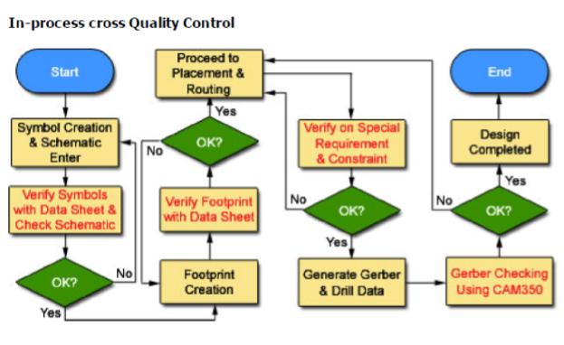
- In-Process Cross QC
Rush PCB’s Design Deliverables:
- Fabrication Drawings
- Assembly Drawings
- Gerber Data
- Drill Data
- Design Database
Design Tools used at Rush PCB:
- Mentor Graphics – PADS
- Altium Designer
- Eagle
- Cam 350
Inputs required for PCB design:
-
- Schematic (soft copy/hand drawn)
- Bill Of Material along with manufacturing part number
- Mechanical drawing/dimensions
- Critical component placement
- Keep-out area
- Specifications of product
- Environment in which pcb is to be fitted
Lead time:
-
- We confirm lead-time only after receiving and confirming all data.
- Our execute simple boards in 2-3 working days
- We can execute moderately complicated boards within 5-7 working days
- For High-Density or complicated boards we take 10-15 working days
Why choose Rush PCB
Rush PCB offers a full range of solutions, and our primary strength is design of Printed Circuit Boards. We define our competitive advantage by the unique perspective of achieving a perfect balance between Science, Art, Logic, and Wisdom.
Rush PCB’s Technical Expertise
With an experience of more than 20+years in the industry, we possess hands-on skills in high speed, high density and high layer count PCB design.
Innovative Thinking
No two PCBs are exactly alike. We customize your products according to your specifications, and this requires creative imagination.
Stringent Protocols
Our streamlined processes ensure that we conform to the best industry standards in developing PCBs.
Quality Assurance
We practice effective quality control measures, including the time-sheet system, prototype evaluation, and Gerber grading.
We Work with a Passion
Rush PCB built not only on talent and skill, but also on passion and commitment. Our genuine love for the job translates into excellent output.
Business Engagement
Rush PCB excels in customer service. We nurture relationships with clients with sincerity and friendship.
I am text block. Click edit button to change this text. Lorem ipsum dolor sit amet, consectetur adipiscing elit. Ut elit tellus, luctus nec ullamcorper mattis, pulvinar dapibus leo.
”Free PCB Design 2-4 Layers”
FAQ
If I do not have a soft copy of the schematic?
We prefer a soft copy of the schematic, as we can easily extract its netlist to reduce the lead time. We also accept hand-drawn schematic as alternative, but this increases the lead time.
Is it necessary to provide BOM along with schematic?
Yes, we require it to determine footprints for placement. We assure you that your data is secure with us. If necessary, we are open to sign an NDA.
What is your lead time for a quote?
We quote only after receiving and reviewing your inputs. If we receive proper inputs as per your requirement, we offer our quote within 12 hours.
Do you take care of Mechanical or housing restrictions?
Yes we do. For this, we require detailed drawing or DXF file from you.
What are the alternatives if the design will not fit in the given size?
Our engineer will be interacting with you at every stage of design, if there is any issue we will assist you in revising your design parameters.
Do you use Auto-Routing?
We use Auto-Routing only to check the feasibility of PCB routing and constraints, and to check whether it is possible to fit the layout within the given size. We follow manual placement according to the flow of the circuit, as this takes less time. However, we manually route DDR bus, differential, and matched impedance traces.
What are your check points for design review?
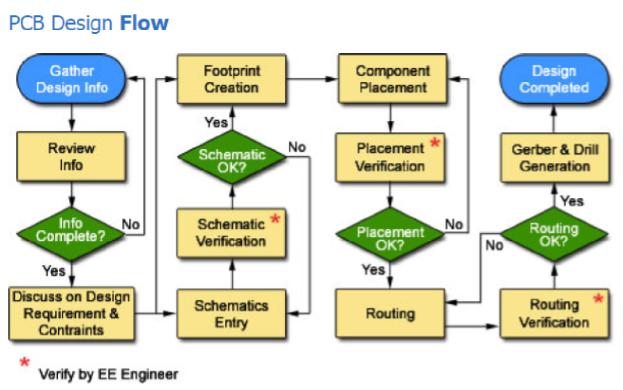
We review the design every stage. Please refer our pcb design flow chart.
Do you take care of DFM?
Yes, our design team always interacts with the FAB team. We follow standard DFM methods.
Do you take care of manual/auto assembly restrictions?
Yes, we use footprints that fit both segments. Our internal assembly house allows us to take care of things easily.
What are the charges for revisions/modifications?
We do not charge extra for minor changes, but we do charge for major changes. We offer our estimates only after reviewing the changes.
What if we have to cancel the order due to revisions?
You still have to pay for the work done.
Do you reverse engineer bare PCBs?
We can reverse engineer simple PCBs along with a schematic. We can confirm only after receiving inputs from you.
Do you take up new ideas or concept projects?
No, Rush PCB engages only with PCB design, fabrication, assembly, and component procurement.
To contact our Business Development team or request more information about PCB layout or PCB Design services, please email us at [email protected] or call us at 1 408-496-6013.