Laser-Drilled Microvias in HDI PCB Manufacturing
Boards keep getting smaller, and components keep getting denser. Traditional BGA routing methods quickly become inadequate as the board becomes more congested. High-Density Interconnect (HDI) technology provides a solution to this issue, and one of the key features of HDI is the use of laser-drilled microvias.
HDI is one of RushPCB’s many specialties. Our capabilities include laser drilling, sequential build-up lamination, copper via filling, and PCB assembly. Your design goes from Gerber files straight to a completed board without being handed off to other vendors.
What Is a Microvia?
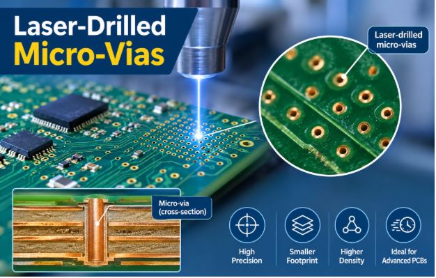
A microvia is a very small, laser-drilled blind via that connects one copper layer to the next. IPC-T-50 defines a microvia as a blind via structure with an aspect ratio of not more than 1:1 and a total depth of not more than 0.25 mm, measured from the capture land to the target land.
A traditional through-hole via connects multiple layers of a board, often extending through the entire board. A microvia connects adjacent layers, leaving other layers available for routing. This is how HDI achieves greater routing density.
Laser Drilling vs. Mechanical Drilling
Mechanical drilling has practical limits when it comes to producing very small holes. As drill diameters decrease, the risk of bit breakage and drill wander increases. Laser drilling avoids some of these limitations.
Laser drilling offers several advantages:
- Reliable Small-Hole Drilling: Lasers can reliably produce much smaller holes than conventional mechanical drills.
- Precise Depth Control: Laser drilling removes dielectric material and can stop at the underlying copper layer, making it suitable for blind microvias.
- Smaller Holes: Smaller holes and capture pads can free up more board space for routing.
- Improved Accuracy: Precise laser drilling and registration support finer-pitch breakout routing for BGA and CSP components.
Sequential Build-Up (SBU): How HDI Boards Are Built
Conventional multilayer PCBs are typically laminated in a single press cycle. HDI boards are often created using sequential build-up (SBU), in which dielectric and copper layers are added one layer at a time. Microvias are drilled, plated, and, where required, filled before the next build-up layer is added.
Bow and warpage can be reduced by maintaining a balanced stackup, including adding build-up layers in pairs on opposite sides of the core.
Common HDI Stackup Structures
| Stackup | Typical Use |
| 1+N+1 | Moderate-density BGAs and cost-sensitive HDI designs |
| 2+N+2 | Smartphones, wearables, and compact industrial controls |
| 3+N+3 | High-pin-count processors, FPGAs, and aerospace and defense applications |
N represents the number of layers in the core.
Every additional lamination cycle adds cost and can increase lead time. Therefore, we evaluate your stackup to determine whether a 1+N+1 structure can meet your requirements instead of a 2+N+2 structure.
Stacked vs. Staggered Microvias
After a microvia has been plated and filled, it may be used as part of a stacked microvia structure. To interconnect three or more layers, designers have two common options.
Staggered Microvias are positioned at different locations on successive layers of the board. They generally offer better thermal-cycling reliability and can cost less than stacked microvias, but they require more PCB real estate.
Stacked Microvias are positioned directly on top of one another and use the least amount of board space. Stacked microvias require careful process control, including reliable copper filling and plating at the via-to-via interfaces, because these interfaces experience additional stress.
When designing a PCB, our general approach is to use staggered microvias when space allows and stacked microvias where routing or breakout requirements demand them. We can help determine which approach best suits your layout and reliability requirements.
Copper-Filled Microvias: Why We Fill Them
Not all PCB fabricators offer microvia filling. At RushPCB, we fill microvias completely with copper, providing several advantages:
- Better Reliability: Proper copper filling reduces the risk of voids and trapped process chemicals that can contribute to failures.
- Better Heat Transfer: Vias help transfer heat away from hot components, and copper-filled vias can provide a more effective thermal path than hollow vias.
- Stackability: A filled microvia provides a solid surface on which to build the next microvia.
- Better Current-Carrying Capability: Solid copper filling improves electrical conductivity and current-carrying capacity.
Via-in-Pad (VIP) for Fine-Pitch Components
For high-I/O components such as BGAs, where space does not allow conventional trace-to-via breakout, microvia-in-pad technology can be used to route component I/O connections.
For via-in-pad to work reliably during assembly, the via must be filled, planarized, and plated over (capped), as described in IPC-4761 Type VII. This creates a flat pad surface that:
- Prevents solder from wicking into the via.
- Helps reduce voids beneath BGA solder balls.
- Supports consistent solder-joint formation during reflow.
Because we provide both PCB fabrication and assembly, the pad flatness achieved during fabrication supports the requirements of our assembly process.
Tips for HDI Microvia Design
These design tips can help improve board reliability and control manufacturing costs:
- Keep the microvia aspect ratio at or below 1:1. Lower aspect ratios generally support more consistent plating.
- Choose the right dielectric thickness. Thinner build-up dielectrics allow for smaller microvias.
- Size capture and target pads appropriately to accommodate laser-to-copper registration tolerances.
- Stagger microvias where possible. Use stacked microvias when routing requirements make them necessary.
- Minimize the number of lamination cycles. Each additional cycle can increase manufacturing costs and build time.
- Specify via filling and capping requirements in your fabrication drawings.
- Consult your PCB fabricator early. A stackup review before layout completion may help avoid costly redesigns.
HDI Applications
HDI technology is used in a wide range of applications, including:
- Medical devices
- Weapons systems and avionics
- Wireless communications
- Vehicle controls
- Consumer and electronic devices
- Industrial controls
Why Choose RushPCB?
- U.S.-Based Team
- One-Stop Shop
- Design for Manufacturability (DFM) Support
- Prototype-to-Production Capabilities
- Engineering Support
HDI PCB Capabilities at RushPCB
HDI Offerings
| Capability | RushPCB |
| Drilling | Laser-drilled microvias |
| Build-up structures | 1+N+1, 2+N+2, 3+N+3 |
| Microvia types | Blind, buried, stacked, and staggered |
| Via fill | Solid copper-filled microvias, as well as dielectric materials like epoxy and resin (which can be plated and planarized) for improved reliability |
| Pad options | Via-in-pad |
| Services | HDI PCB fabrication and assembly |
Frequently Asked Questions
What Is the Difference Between a Microvia and a Standard Via?
A microvia is a small blind via, typically laser-drilled, with an aspect ratio of 1:1 or less and a depth of no more than 0.25 mm under the IPC-T-50 definition. Standard vias are often mechanically drilled and may extend through the entire board or connect other combinations of layers.
What Is a 1+N+1 HDI Stackup?
A 1+N+1 HDI stackup consists of a multilayer core (N) with one sequential build-up layer on each side. Microvias connect the outer build-up layers to the adjacent inner layers.
Are Stacked Microvias Reliable?
Yes, stacked microvias can be reliable when properly designed and manufactured, with complete copper filling and tightly controlled fabrication processes. Where space permits, staggered microvias can offer better thermal-cycling reliability.
Why Should Microvias Be Filled?
Filling microvias can improve reliability, support heat transfer, enable via stacking, and provide a flat surface for via-in-pad applications.
When Is Via-in-Pad Required?
Via-in-pad is often used for fine-pitch BGAs and other high-density components where there is insufficient space to route signals from component pads to conventional vias. Whether it is required depends on the component footprint and routing constraints.
Does HDI Increase the Cost of a PCB?
HDI boards typically cost more than standard PCBs because of laser drilling and additional lamination cycles. However, HDI can reduce the overall system cost by enabling smaller boards and, in some designs, fewer total layers.
Does RushPCB Assemble HDI Boards?
Yes. RushPCB provides HDI PCB fabrication and assembly, offering customers a single-source partner from bare-board manufacturing through assembly and box-build services.
Ready to Build Your HDI Board?
RushPCB can help you take advantage of laser-drilled microvias for both prototype and production builds. Simply send us your Gerber files and layer stackup for a design-for-manufacturability (DFM) review and quote. Our team will review your requirements and contact you with the next steps.