

High Density Interconnect or HDI PCBs offer more functionality within the same or a smaller area. At Rush PCB, we use the latest technology for increasing the use of HDI in computer products and mobile phones. Using HDI PCBs has resulted in revolutionizing the electronics industry with several new products such as 4G communications and touch-screen computers. It even benefits avionics and is useful to the military, such as in intelligent military equipment.
As the name suggests, HDI PCBs come with high density properties. Primarily made of high-performance thin materials, HDI PCBs contain thin traces packed close together, and laser micro-holes, giving them the high density for supporting more functions per unit area. These high technology high density boards contain multiple stacked copper layers interspersed with micro-holes that help designers create more complex interconnections. High-technology products and mobile devices using large fine-pitch high-density chips benefit from the complex structures of HDI PCBs.
Architecture of HDI PCBs
It is possible to have one or more high density interconnect layers within a PCB. These can have stacked or staggered micro-holes, and more challenging designs can have multilayer stacked copper filled micro-holes.
More advanced architectures can have arbitrary HDI layers in a PCB, including all layers as HDI. Copper tracks present on any layer of the PCB can connect to copper tracks on any other layer through multi-layer stacked copper micro-holes. This structure offers a reliable interconnection for highly complex fine pitch SMT components, such as COB and BGAs.
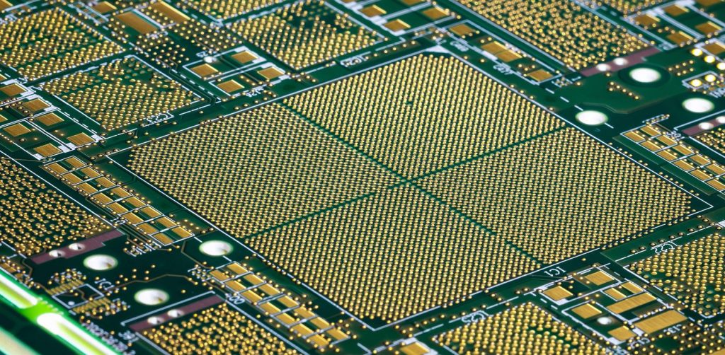
Fig 1: Example of HDI PCB
Rush PCB makes micro-holes using laser drilling. Typical diameters are 100 microns (0.004” or 4 mils), 125 microns (0.005” or 5 mils), and 150 microns (0.006” or 6 mil), and the fabricator aligns them optically with pads of diameter 200 microns (0.008” or 8 mils), 250 microns (0.010” or 10 mils), and 300 microns (0.012” or 12 mils) respectively. This alignment allows achievement of greater routing density.
Rush PCB uses interleaved micro-hole structures for routing fine-pitch components with 0.5 mm pitch. However, for components with still finer pitch such as micro-BGA with 0.4, 0.3, or 0.25 mm pitch, we use stacked micro-holes using the inverted pyramid routing technology.
Importance of Micro-Holes
PCB manufacturers use the micro-hole technology to improve the routing density of their boards without increasing the cost massively. Although many customer requirements are important, for instance quality, reliability, design rules, and more, the choice of a micro-hole process and the manner of filling it lies with the fabricator, who must select the process to optimize the PCB manufacturing process. This selection depends on:
- Laser drilling of micro-holes
- Plugging the buried holes
- Outer plating
- Transfer of graphics
- Electrical tests
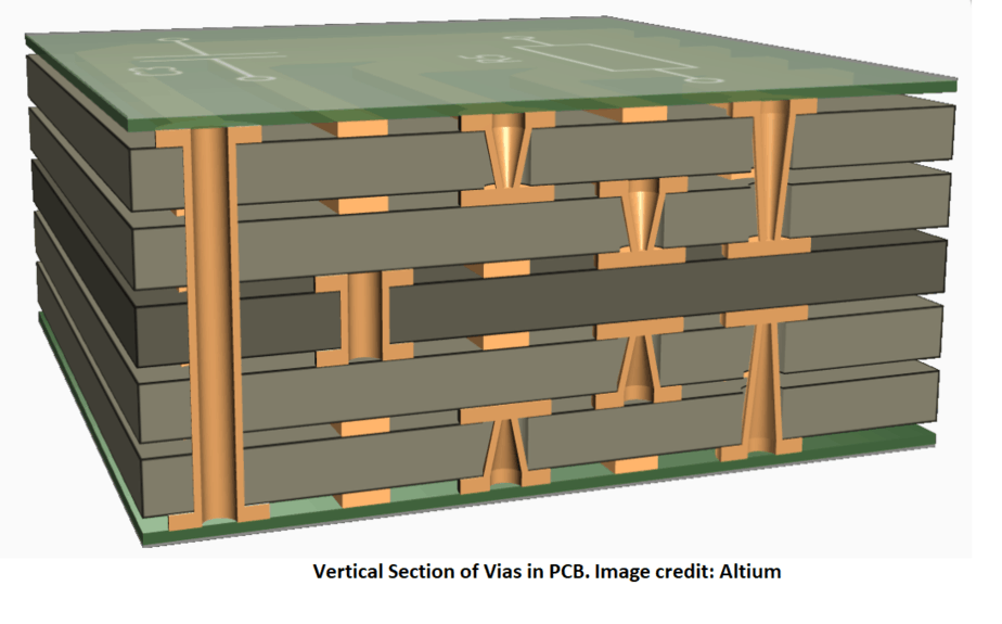
Fig 2: Example of Micro-Holes
Although the quality and efficiency of the above processes are individually important, the coordination between them is even more important to achieve the final product quality. Among all the above, plugging the micro-holes is the most important, and fabricators consider this as the key process in mass production of PCBs with micro-hole technology.
Why Plug Micro-Holes
Plugging micro-holes leads to several advantages. Some of them are:
Cost Reduction: Rush PCB uses cost-effective liquid epoxy resins for plugging micro-holes on PCB layers. Making micro-holes does not require small and expensive drill bits. Micro-holes also do not require using resin-coated copper foils that usually have a limited hole filling capacity. It is possible to use thin copper foils, without reducing the reliability of the PCB.
Routing Density: Controlling the thickness of copper on the inner layers of the PCB allows Rush PCB to fabricate the thinnest traces. We place the micro-holes on the annular pads of the inner vias after plugging them. We ensure the flatness of the outer surface to allow processing thin traces. We can place micro-holes directly on the traces so that they do not need any pads on their bottom. All this increases the routing density on the layer.
Reliability: For plugging the micro-holes, Rush PCB uses plugging materials chosen specifically by matching their CTE or coefficient of thermal expansion. This allows the inner layers to have vias with wall thickness reaching 25 microns. Not only does this improve the reliability of the vias in the inner layers, the overall reliability of the PCB also improves, even when it has very thin traces. Reliability tests by Rush PCB shows that such plugging does not cause any cracks or defects in vias even when the board has gone through 1000 cycles of heat cycle test ranging from -55 °C to +125 °C.
Advantages of Micro-Holes
Micro-hole and HDI technology allow OEMs to achieve smaller, lighter, flatter, and more portable products. As the SMT component technology progresses and adds new geometric shapes such as flip chip and chip level packaging with pitch reducing to 0.5 mm and less, it becomes increasingly impossible for traditional PCB technology to route boards with such advanced components.
With HDI as the new PCB manufacturing process, designers can reduce the size of pads to 200 microns (0.008” or 8 mils). However, it is impossible to use mechanical drills to make holes in these pads, as the hole size necessary is 100 microns (0.004” or 4 mils). This is where the micro-hole technology comes in, as lasers can drill such small holes easily and cost-effectively.
Micro-holes have a reduced aperture, allowing the elimination of a large number of fan-outs for BGA components. Moreover, it is possible to place micro-holes directly on the pads, increasing the routing density. One of the direct advantages of using the micro-hole technology is a reduction of total number of layers, effectively reducing the stack height of the PCB, and hence, its cost.
Rather than use buried vias that require plating, HDI PCBs with buried micro-holes are more cost-effective, since micro-holes only need plugging with special purpose material.
Conclusion
Micro-holes in the inner layers of PCBs offer several advantages to PCB designers and manufacturers. Rush PCB has been able to reduce manufacturing costs substantially by using plugged micro-holes and HDI technology for PCBs. This is more significant when the PCB has a large number of vias.


