

The electronic components manufacturing industry has been developing several types of fine-pitch components in recent years. These ultra-small integrated circuits include packages like FC, CSP, BGA, TOFP, VSOP, SSOP etc. The printed circuit board or PCB industry has followed the development of such components with fine-pitch boards. Rush PCB is gradually increasing application of BGA, CSP, and FC packages in PCB assembly, following the mature technology, convenient packaging, and low manufacturing cost of these packages.
As SMT is now mainstream for the electronic PCB assembly, the trend is towards thin assembly, high reliability, small size, and easy automated production. Eminent high-tech PCB manufacturers such as Rush PCB have experience in testing surface mount PCBs, and have extensive experience with fine-pitch components like Ball Grid Arrays or BGA, Chip Scale Packaging or CSP, and Flip Chip or FC packages.
The signal transmission path is shorter in CSP and FC packages, as the packaging density is high, feature sizes are smaller, and there is significant reduction in the overall area. As the flip-chip is nearly the same size as the chip die, it does not actually have a package, it has the advantage of highest density and small size, and this allows signals to travel at extremely high speeds, with enhanced electrical performance. The advantage for OEMs is the significant reduction in package size brings down the PCB assembly size and the product size considerably.
Flip-Chip PCB Assembly
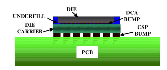
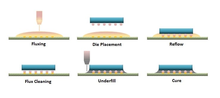
Assemblers typically mount a single flip-chip on a medium-sized board. Usually, this is an expensive PCB, as the CTE or coefficient of thermal expansion of the board must match with that of the flip-chips. If left unmatched, different expansion rates may cause movements leading to bending and weakening of interconnections between the chip and the PCB assembly board.

Fig 1: Flip-Chip Assembly Process
To strengthen the interconnection, assemblers usually fill the space between the chip and the PCB with epoxy resin. This helps to spread the stress and thereby protect the interconnections.
Multi-Chip Modules
Assemblers put the flip-chip or other fine-pitch components such as BGA on a substrate, also known as MCM or multi-chip module. The substrate can hold multiple integrated circuits and the assembler assembles them as a single device. Therefore, the MCM behaves like a single component and handles an entire function.
Usually, the substrate of the MCM has various components, with the bare dies of the substrate connecting to the surface via wire, flip-chip, or tape bonding. The assembler them encapsulates the module with a plastic mold and mounts this on a larger PCB. MCMs offer improved performance, reducing the size of the device considerably.
There are several advantages of using MCMs. After underfilling, if the assembler tests the MCM and finds the flip-chip mounted on it non-functioning, they can scrap only the MCM and not the entire PCB.
Chip-Scale Packaging
CSP or Chip-Scale Packaging technology makes it easier to mount or unmount packages compared to flip-chips. Moreover, for CSP assemblers do not need to fill the gap between the PCB and the chip with epoxy. They can also use standard SMT production equipment for using CSP.
Testing Fine-Pitch Component Assemblies
The competitive environment in the electronic industry makes it necessary to test each PCB assembly board, irrespective of the density and variety of technologies assemblers use. Testing is necessary for meeting demands of high efficiency, product reliability, and process control. For inspecting and testing flip-chip and CSP board assemblies, Rush PCB uses several technologies including functional inspection, automated X-ray, and on-line inspection with in-circuit testing.
Among these, the ICT or in-circuit tester is one of the most basic electrical test equipment the PCB manufacturers use. ICTs typically detects PCB solder joints for open and short-circuit faults, and points to the component or location of the fault. However, with density of circuit boards on the increase, and the prolific use of fine-pitch components, assemblers are beginning to use boundary scan technology instead.
Assemblers also use Automated X-rays for inspecting assembled boards. X-rays passing through boards generate an image that makes it easy and intuitive for analyzing PCB solder joints and detecting defects. Manufacturers can use X-rays to detect faults in double-sided circuit boards mounted with components. Moreover, it is also possible to inspect slices of images of multi-layer PCBs, and view invisible solder joints of BGA chips. Using automated X-ray inspection equipment, it is possible to inspect dense, fine-pitch PCB assemblies. X-ray inspection is an advanced test method and assemblers use for quality control of SMT production lines.
Advantages of Flip-Chips and CSPs
FCs and CSPs are refine solutions offering low-cost packaging for improving the characteristics of electronic devices by saving space on a PCB assembly. These improved packages have infinite development prospects. The PCB manufacturing industry is keeping pace with these advanced packaging technologies by developing new fabrication technologies such as HDI or High-Density Interconnect boards. They are diversifying into advanced inspection technologies as well.
Apart from online testing for PCB components, manufacturers are also using functional testing through SAMD or Scanning Acoustic Microscopy and Detection methods, Automated X-ray testing, and more. This is greatly improving the quality of the SMT assembly process.
Conclusion
Rush PCB is moving towards zero-defect manufacturing for SMT assembly, with most assembly manufacturers following the goal of pass rate. Rush PCB uses automated X-ray testing for focusing mostly on the quality of PCB solder joints, and ICT for deciding on the value and orientation of the SMT component.


