

Rush PCB assigns great importance to the correct sizing of PCB traces during PCB design. This involves not only the PCB trace width but several other important factors as well, like trace length and style.
Importance of Trace Width
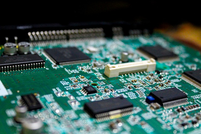
PCB traces connect all kinds of electrical signals from one junction to another. The signals may be analog, digital, or power. Junctions may start from the pin of a component, branch off another trace, a pad, or a test point. Designers use mils to measure the trace width, and one mil represents one-thousandth of an inch. In metric terms, designers measure the trace width in microns, with one micron representing one-millionth of a meter.
In practice, trace widths may vary from 5 to 12 mils (125 to 300 microns) for ordinary signals when there are no special requirements. However, designers must consider many aspects while defining the length and width of a trace for a specific application.
When choosing the trace width and type during a PCB design, designers must also consider and balance the printed circuit board fabrication cost, board density and size, and the signal integrity. For specific board requirements like noise mitigation, optimum coupling, signal integrity, high voltage, and high current, it is more important for the designer to meet them through PCB design rather than optimize the manufacturing cost or the overall board size.
Specifying PCB Traces During PCB Fabrication
PCB fabrication costs rise with tighter PCB specifications and tolerances. This is because manufacturers and inspectors need high-end equipment for both fabrication and testing of boards. Specifications leading to higher costs in PCB fabrication are:
- Trace width and spacing less than 5 mils (125 microns)
- Vias with hole diameter less than 8 mils (200 microns)
- Trace thickness differing from 1 oz (1.4 mils/36 microns)
- Traces with defined impedance, differential pairs, and controlled lengths
Many designs require the above specifications or better. This is specifically true of high density interface or HDI boards. High density boards may incorporate parallel buses with high signal count or close-pitch components such as BGA. The trace widths in such boards may be as thin as 2.5 mils (63 microns). They may have laser-drilled micro-vias with 6 mils (150 microns) diameter or less.
At the other end of the spectrum, high-power designs may require very wide traces or planes covering the entire layer, with higher copper weights than normal.
PCB design with space constraints may need board thickness to be very low, along with several layers, each with limited copper weight.
Other printed circuit board designs may need controlled impedance traces for high-speed communication from one peripheral to another. To minimize inductive coupling and reflections, the traces may have to be of a certain length and style.
High voltage PCB designs may require a specific spacing between two differential signals to preclude the possibility of arcing between them.
In general, a printed circuit board may contain a variety of trace widths, as they carry different signals. General purpose digital signals are usually thin traces as they have no special requirements for conducting high power or noise mitigation. Traces carrying high currents may have to be wider and thicker depending on the amount of power they handle.
Calculating PCB Trace Width
It is necessary for the designer to calculate the trace width and length when the trace must carry a power signal from one point on the board to another. This is necessary as the traces on a PCB act as resistors. The longer and narrower the trace, the more resistance it has. Unless properly designed, high currents through the trace can cause a significant voltage drop, heat up the trace, and in extreme cases may even damage the trace by melting it. Therefore, depending on the trace resistance, the designer must calculate the optimum trace width and length for carrying the current with the expected voltage drop.
There are two ways designers can make the calculations:
- Using Equations
- Using PCB Trace Width Calculators
Using Equations
The equations are meant for calculating PCB traces on external layers. There are two equations, one for calculating the cross-sectional area of the trace, and the other for the width, using data from the first equation. IPC guidelines offer values for various constants in the equations.
A third equation is necessary for calculating the resistance of the trace depending on its length. The voltage drop is then proportional to the calculated resistance.
Using PCB Trace Width Calculators
It is possible to use IPC-2221 generic standards on printed circuit boards design for estimating the PCB trace width for different current handling capacities. Various graphs are available, classified for internal and external conductors.
The graphs show the relationships between variables related to trace width—cross-sectional area, temperature rise, and maximum current carrying capacity—for traces on both external and internal layers. Two graphs are in common use:
- Current vs. cross-sectional area for various temperature rise
- Conductor width vs. cross-section for various copper weights
Digital Trace Width Calculators
Trace width depends on several factors like thickness of copper layer or copper weight, length of trace, position of the trace in the stackup, and so on. Therefore, making accurate calculations manually is a difficult task. PCB manufacturers provide digital tools to calculate trace width.
Digital trace width calculators are tools that take various factors mentioned above into consideration, and provide an accurate value for the trace width required.
Importance of Trace Length
Many electronic equipment are now trending with reduced form factors, and circuits operate at low voltages. Temperature rise and voltage drops are the most dominant concerns in such designs. While calculating the track width is important for limiting the temperature rise, knowing the trace resistance is important to decide whether the voltage drop at the end of the trace is within allowable limits.
Temperature rise will not change by making trace longer. In fact, the longer a trace is, the more surface it has for dissipating the heat it is generating. However, the resistance of a trace increases with its length, and ignoring the trace length can cause a severe drop in voltage.
Conclusion
Rush PCB recommends that printed circuit board designers verify the current carrying capacity of their PCB traces instead of using estimated widths. They can use the various tools available online for calculating the necessary trace width whether their trace is on an internal layer or on an external one. For low-voltage designs, they should also check the voltage drop along the length of the trace, and increase the width for reducing the drop.


