

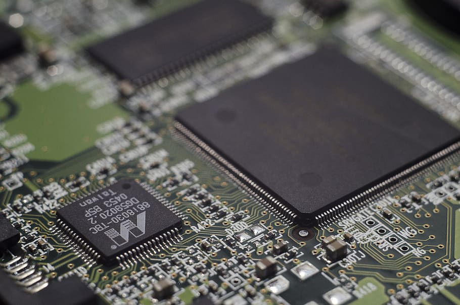
Rush PCB places great emphasis on proper PCB etching techniques, as etching is one of the most important processes in PCB manufacturing. PCB manufacturers use etching to decide the amount of copper remaining on the laminate, Etching defines the copper lands and traces that make the circuit on the laminate.
PCB manufacturers use copper clad laminates to fabricate circuit boards. They transfer an image of the circuit on the copper, and use chemicals to remove or etch away the copper part not covered by the image. This is the chemical etching process. Although it is possible to use a non-chemical process like milling to remove the unwanted copper from the laminate, this is not suitable for forming fine lines and spacing.
Different Types of Etching Techniques
Three types of etching techniques are in general practice:
- Subtractive Technique
- Additive Technique
- Reactive ion Etching Technique
While the subtractive technique is more common, it is suitable for general purpose circuit boards only. The additive and reactive ion etching techniques are essential for high density interconnect (HDI) boards and flexible boards.
Subtractive Technique
This method of etching removes unwanted copper from the copper clad laminate by dissolving the copper chemically. The fabricator applies a photosensitive resist material in the form of a dry film on the copper foil. They place a negative circuit pattern on the film, and expose the combination to UV light. The UV light passes through the transparent parts of the pattern and interacts with the resist material to fix it. When developed with the necessary chemicals, the unexposed resist material washes away, leaving the circuit pattern on the copper foil protecting the traces, pads, and vias.
The fabricator then places the board in the etchant solution to dissolve the exposed copper not covered by the resist. Finally, the fabricator removes the dry film material from the board, leaving the copper traces on the surface.
Advantages of the Subtractive Technique
- Suitable for producing copper pads around non-plated through holes that connect to large copper areas like ground.
- Suitable for producing boards that have a large residual copper ratio.
- Low manufacturing costs and short process flow times.
Disadvantages of the Subtractive Technique
- Cannot produce plated through holes with very small copper pads or no pads at all.
- Cannot produce very fine lines closely spaced.
- Cannot produce traces and spaces with tight tolerances.
- Difficult to control the straightness of trace edges
- Difficult to control the level of etch undercut.
- Not suitable for printed circuit boards with heavy copper.
Additive Technique
The additive technique for printed circuit board manufacturing uses two common technologies:
SAP — uses a thin layer of electroless copper (0.1 um to 1.0 um) over the substrate
mSAP — uses a thin layer of laminated copper (0.1 um to 1.0 um) over the substrate
Both SAP and mSAP processes follow a similar process where the PCB manufacturer coats a thin layer of copper on the substrate. Then they deposit a photoresist of negative pattern of the design on the copper using the photolithographic technique, and electroplate the uncovered copper to the desired thickness. Next they remove the pattern deposition and the seed copper.
The catalytic photoresist ink for depositing the pattern controls the horizontal dimensions of the line width and spacing. The additive process that deposits electroplated copper on the desired pattern controls the vertical dimension of the copper thickness.
Advantages of the Additive Technique
- Suitable for very fine lines (about 5 um) and spaces.
- Suitable for both rigid and flexible substrates.
- Costs are very competitive.
- Both holes and traces can be plated together.
- Transition from trace to hole is smooth and seamless.
- Copper surface is of high quality, smooth, and rounded facilitating high frequency and high speed signals.
- Overcomes all disadvantages of the subtractive technique.
Reactive ion Etching Technique
This is a directional PCB etching process that utilizes ion bombardment for removing unwanted copper from the board. PCB manufacturers use this micro fabrication process for fabricating very fine lines and spaces on printed circuit boards. They use a chemically reactive plasma in a vacuum chamber for aggressively etching in a vertically downward direction. Minimized horizontal etching leaves clean and accurate corners.
For ensuring a uniform etch, it is necessary to control the ion density, electron temperature, and the plasma potential. Fabricators commonly use carbon tetrafluoride and oxygen gas for the etching.
Advantages of the reactive ion etching are the same as those for the additive technique. It is possible to achieve a faster etching rate by raising the temperature and pressure of the chamber during the etching process.
Uses of High Quality PCB Etching
The most visible markets utilizing the additive and the reactive ion printed circuit board etching techniques are the smartphone and computer motherboard markets. Apple started the trend and other manufacturers have quickly adopted the technology. Current designs blend a combination of layers that use subtractive etching with layers that use the high quality etching technology.
Using the mSAP technology allows fabricators to make thinner and smaller smartphone motherboards. This allows designers to add a larger battery, extending the battery life for consumers. Although the present design allows for 30 microns trace and space dimensions, future designs are targeting 10 microns.
Once smartphones had proven the concept of blending layers using the subtractive process with those using the high quality etching process, manufacturers are also spreading the concept to other markets such as wearable, medical devices, medical implants, automotive, aerospace, and defense markets. For instance, manufacturers can move from 10-layer HDI designs with four lamination cycles to a design using 6-layers of single or double lamination design.
Applications using high quality PCB etching
PCB applications that need extremely thin copper, those concerned with space and weight, and applications that use complex pin-outs are the ones using the high quality PCB etching techniques like additive and reactive ion etching.
For instance, many medical implants use 20-micron trace and space in their PCB boards, along with double-sided design, and gold conductors on polyimide substrates. The presence of gold ensure biocompatibility.
Military and aerospace applications typically require high density interconnect designs with tight pin outs, finer lines, and very small vias. Most designs in these fields use stackups similar to those in smartphone designs. PCB manufacturers reduce expensive lamination cycles and layer counts by judicious integration of layers using SAP and mSAP technologies with layers using the simpler subtractive etch technology.
Wearables are another set of devices making frequent use of the high quality PCB etching techniques. Using the newer technologies ensures that wearables successfully meet requirements of thinner forms, lighter weight, and high flexibility.
Conclusion
Rush PCB finds the traditional subtractive etch technology is incapable of meeting the advanced requirements of electronic devices with their smaller and thinner form factors and higher functional requirements. The present requirement for the latest equipment and processes, especially in complex HDI printed circuit board designs, is newer technologies for achieving sub-25-micron line and space. In PCB boards manufacturing, the current trend is moving from the traditional subtractive process to the high quality PCB etching techniques like additive and reactive ion technologies.


