

Designers using BGA or Ball Grid Array ICs need HDI or High-Density Interconnect PCBs to make the most effective use of these high-density packages. Using multiple BGA components, when some of them are high pin count types, requires special routing techniques, known as escape routing strategies, for routing traces to connect to and from the balls or pins under these components. Rush PCB has a rich experience in designing HDI PCBs with BGA. We understand it can be difficult to design escape routing under high pin count situations where the BGA also handles high speed or high frequency signals. This is because the escape routing must also maintain controlled impedance requirements.
When Rush PCB designers plan an HDI board, the escape routing they will use depends primarily on the pitch of the on-board BGA component. This defines the maximum trace width they can use between the solder pads. The minimum trace width depends on the manufacturing capabilities, the layer stack, and the necessary impedance. Here we will discuss the considerations when selecting the escape routing strategy for HDI and BGAs handling high speed signals.
Escape Routing Strategies
For HDI PCBs with moderate layer counts, the escape routing strategy that Rush PCB designers prefer for fine-pitch BGAs is neck-down as they route the traces into and out of the BGA. The first row of solder pads on the board requires routing of exterior traces directly onto them. For the second row, the designer must reduce the trace width a little to allow them to pass between the first row of pads. For the remaining pads, the designer must use an interior layer for the traces to reach them. According to Rush PCB, it is generally possible to route two rows in each signal layer for maintaining cross-talk limits and controlled impedance.
Dog Bone Fanout Strategy
Beyond the first row of pads, the nature of routing depends mostly on the pitch of the BGA, the necessary trace width, and the size of the micro-via the designer will use. Accordingly, the dog bone fanout is the is most popular BGA escape routing strategy designers follow. The dog bone fanout has a pad placed very close to the actual pad for the BGA pin/ball, with a short trace connecting the two pads. The second pad has a via for the trace to continue to another layer. As the track connecting the two pads has a solder mask covering it, the via, despite being on a pad, does not need plating or filling. However, this dog bone fanout strategy is suitable only for BGAs with pitch of 1 mm, and designers can extend it to 0.8 mm BGAs at the most.
Micro-Via Strategy
BGAs with pitches less than 0.8 mm will have smaller pad sizes, including their annular ring. As regular vias will be too large for these pads, the designer must use laser-drilled micro-vias to allow the traces to reach the inner layers. The difference between a regular via and a micro-via are significant in two aspects:
Aspect Ratio: For a via, the aspect ratio is the via length divided by its diameter. For a micro-via, designers maintain the aspect ratio below 2, which means the via length will be less than twice its diameter. For instance, for a standard board of 32 layers, with a 2-layer core and layer thickness of 2 mil, the diameter of the micro-via cannot be less than 1 mil. For boards with higher layer counts, Rush PCB maintains the aspect ratio of a micro-via very close to 1.
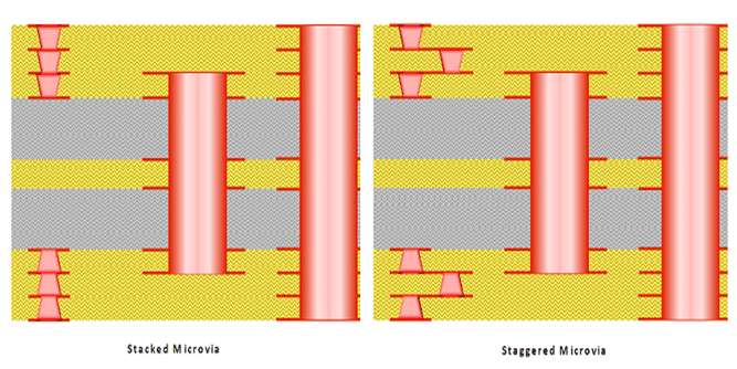
Via Depth: Although regular vias often span the entire thickness of the PCB, their presence reduces the real estate for routing traces, leading to an increase in stack height. Therefore, designers resort to using blind and buried vias that span one or two layers at the most, while stacking them to reach the other layers. Similarly, for HDI boards with high layer counts, designers use micro-vias that span only a single layer. For extending to other layers, designers use stacked or staggered micro-vias.
Mechanical Drilling Vs. Laser Drilling: Mechanical drilling is reliable only down to about 8 mils, as drill breaking pushes up the cost per hole below this size. Additionally, mechanical drilling is a slow process that limits the throughput. Laser drilling overcomes the above limitations of mechanical drilling, and reduces the cost per board.
Read About: INTRODUCTION TO DRILLING AND VIAS
Using dog bone fanout for a BGA with 0.8 mm pitch requires trace widths of about 10 mils. Micro-vias for these traces must be of 6 mil diameter or less. For BGAs with pitch close to 0.5 mm, Rush PCB designers use 7 or 8 mil traces that allow adequate clearance to nearby pads, along with micro-vias-in-pads for routing into inner layers.
The advantage with micro-vias is they allow stacking, irrespective of the strategy the designer follows for achieving necessary routing density. Rush PCB conforms to the IPC 6012 standard for ensuring maximum reliability when using micro-vias. We use both stacked and staggered micro-vias as necessary.
Controlled Impedance
Impedance is a significant factor when the BGA must handle high speed signals. Impedance control is necessary as a fanout section connects to a longer trace that terminates to a receiver. The length of the trace along with the parasitic inductance and capacitance of the micro-via affects the impedance of the fanout portion.
Rush PCB recommends ignoring the fanout portion if the length of the trace is shorter than the wavelength of the high-end digital signals the BGA is handling. For instance, for a digital signal of 20 GHz, a 0.73 mm stripline is critical when using an FR-4 substrate. Therefore, components with high pin count and handling high speed signals will typically require impedance control during fanout. For boards with higher layer count, the designer must reduce the trace width to compensate and maintain the impedance to specific value.
Conclusion
Although HDI PCB design can be difficult, Rush PCB uses proper escape routing strategies for optimizing the design. We use cutting edge technology to design modern HDI PCBs for major electronic companies. Our customers range from computer systems to defense and aerospace systems to power electronics. We make sure your PCB is fully manufacturable before we start, and you only have to give us a call.


