

The electronics industry defines fine-pitch PCB assembly as those with a significantly high number of components per unit area. That means the components on the board are very close to each other, bordering on the tolerance limits of the fabrication processes. Rush PCB advises following some simple rules of thumb that makes it possible to successfully execute such high-density PCB assemblies.
Fine Pitch Circuit Boards Must Pass DFA
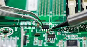
High-density circuit boards generally also require fine-pitch components, pushing up the capabilities and cost of fabrication. As the component density increases, their physical size decreases. Smaller components require smaller pads, and consequently, the accuracy of the pick-and-place machine increases proportionately. Use of grid-array and leadless components is very common, requiring X-ray inspection during their assembly.
To meet and conform to Design for Assembly or DFA requirements, designers must be aware of the equipment and capabilities of their contract manufacturer. Failing which, there must be a close relationship between them. Contract manufacturers usually have considerable experience, with the capability of providing designers with suitable guidance for fine pitch circuit board design.
Rush PCB has experienced engineering and support teams that work with customers every step of the way for ensuring results of the highest quality—both for PCB manufacturing and assembly.
Fine Pitch Circuit Boards — the Challenges
The biggest challenge a designer faces is laying out hundreds of components within a limited space, while following the signal and power flow, and maintaining signal integrity. At the same time, the designer must allow adequate space for routing traces, and introduce power planes to shield sensitive circuits, while allowing them to carry adequate amounts of current to all parts of the board. For doing all this, the designer must follow some rules:
Selecting the Component: Before starting the PCB layout, the designer must select components that are adequately small. Surface mount technology or SMT components come in a large variety of forms and the designer must select the proper size that will save significant board space. Ultimately, the designer must balance the fabrication costs with the savings made for the board space.
Although the designer can save significant amounts of space by using fine-pitch components, the cost of assembly can go up. This is specifically true for components requiring special tools for inspection, such as for grid-array components that offer a pitch of 0.3 mm between pins, but require X-ray inspection after assembly.
Tighter tolerances and be expensive. Therefore, designers looking to remain within a certain budget may find selecting larger components as best approach. IC manufacturers offer the same component in various packages, so the designer must only study the data sheets and pick the right format for building up the Bill of Materials or BOM.
Component Ratings: While high densities will typically reduce the PCB space required, the designer must also consider the rating of each component. The designer must balance the safety margin for each component against its size, as smaller components may only be available only in low power or voltage ratings.
For instance, for a power rail of 10 V, using a capacitor rated for 50 V may be an overdesign. However, a capacitor with a 10 V rating, although a very small size, may not have enough safety margin. Therefore, the designer would be better off with a 16 V capacitor, with a slightly larger size, as it offers greater reliability.
Size of the Board: Once the designer consolidates the schematic and the BOM, they can define a reasonable size for the board—as a starting point.
In most cases, mechanical constraints, like the space within the cabinet housing the PCB, restricts the physical size of the board in the X, Y, and Z dimensions. The process becomes easier when the mechanical designer has not yet frozen the details, and the PCB designer can negotiate the dimensions of the board.
Most high-density designs allow the board size to dictate the mechanical hardware surrounding it. Therefore, the mechanical designer will wait for the PCB designer to verify that they can achieve the size of the board.
The PCB designer must first accommodate all the connectors on the PCB at specific locations, as these must interface with other related connectors outside. Next come the bulky components, as they may have height restrictions. Large ICs require adequate space around them for routing breakout signals. Some components may generate interference, while some may be susceptible to that interference, which means, there must be as much separation between them as possible. Routing must take care of cross-talk and isolation between traces. The designer must maintain signal integrity for sensitive signals by enclosing them within copper planes. The fabricator may have restrictions on how close to the edge the designer can place components and traces.
After completing the preliminary check, the designer must define proper design rules for the layout. For this, it is necessary to discuss fabrication capabilities with the contract manufacturer.
At this time, there will be several trade-offs to consider for achieving the budgeted cost of the PCB. Rush PCB offers several options that help customers achieve their cost targets by balancing capabilities. For achieving target costs, it is necessary that the designer and contract manufacturer set the appropriate design rules at this point.
For instance, the designer may determine that a fine-pitch IC with 0.3 mm pitch suits the PCB, but the contract manufacturer’s capabilities can only fabricate with 0.4 mm. In such cases, either the designer changes the IC form factor or looks for another contract manufacturer with better capabilities. Similarly, the designer must ascertain the contract manufacturer can handle the impedance controls and differential pairs they are planning on using.
Component Layout: After placing the design rules in place and understanding the contract manufacturer’s capabilities, the designer can proceed with the component layout. They must fit the components as close together as possible, with adequate space in between for traces and vias—this being largely a trial and error process.
Designers may have their own preferences, with some starting with laying out the high-power components first, as these traces require calculated widths. Isolated components come next, followed by fine-pitch components and high-speed circuits.
During the above exercise, it is common for the board size to grow or shrink in either the X- or the Y-direction or both. Designers use additional considerations for optimizing space in high-density designs.
Optimizing Fine Pitch Circuit Board Designs
Tooling Holes: The contract manufacturer requires these holes for assembly and testing. Fabricators use these holes to align the PCB for drilling holes, stencil placement, pick-and-place machines, and text fixtures. The designer must be aware of the contract manufacturer’s requirement for tooling holes.
Via-in-Pads: Although once considered bad for design, designers now use via-in-pads specifically for reducing space for routing breakout traces from fine pitch ICs. The difference is, these via-in-pads are of the filled or tented type to disallow solder wicking.
Fiducial Marks: Although not strictly helpful in deciding the board size, fiducial marks help by increasing the accuracy of pick-and-place machines when they are placing fine-pitch components, thereby improving the reliability of the assembly. Designers use a couple of 1 mm circles as fiducial marks on the top copper layer on opposites of fine pitch ICs. PCBs without fine pitch ICs may have two fiducial marks on opposite corners of the board.
Test Points: For help in testing the PCB assembly, designers preferably add test points on traces carrying important signals. It is important to detect assembly errors and at times, testing is the only option for detecting them. Test points help in detecting shorts and opens within multi-layered PCBs, as these are not visible from outside.
Conclusion
Designing for high-quality fine-pitch PCB assembly is always a compromise between cost and complexity. The trade-offs outlined by Rush PCB can save our customers considerable time and money during the development of high-density PCBs and their assembly.


