

Printed circuit boards (PCBs) getting increasingly more complex, and this is evident from the mixed-performance that OEMs demand from them. These requirements lead to a diverse set of highly sensitive components PCBs feature, with shrinking real estate cramming them on the board. It is important these components are compatible and the PCB manufacturable. According to Rush PCB, these requirements make rigorous PCB assembly inspection and testing procedures unavoidable, especially in the prototyping stage where flexibility and speed are essential.
Importance of Inspecting and Testing PCBs
At Rush PCB, we deliver high-quality products to our customers. For this, we ensure inspection and testing throughout the PCB assembly process. We place a major emphasis on prevention, rather than fixing the defect with rework. The most common types of inspection and testing methods that Rush PCB follows during PCB assembly are:
- Optical Inspection
- X-Ray Inspection
- Technological Inspection
- Electrical Performance Inspection
- In-Circuit and Functional Testing
- Burn-In Testing
The industry classifies PCBs into rigid and flex types, and these can be single-sided, double-sided, and multi-layered. The industry also classifies PCBs according to their quality—Class 1, Class 2, and Class 3—with Class 3 being of the highest quality.
Differences in quality among PCBs results in differences of complexity in inspection and testing methods. Post PCB fabrication, the manufacturer carries out inspections to determine if they have achieved the quality specified by the design requirements. As the PCB moves towards assembly, the assembler takes up further inspections and testing procedures at different stages to ensure good product quality.
Optical Inspection
At Rush PCB, depending on the assembly levels of production, we use one of two types of optical inspection methods—manual and automatic. Manual methods of optical inspection are more suited to low levels of assembly, such as for sample and prototype runs. For high levels of production, we prefer automated optical inspection (AOI). Assembly stages where the optical inspection methods offer substantial benefits are immediately after SMD placement and after completing reflow soldering.
Manual Optical Inspection: Instruments involved in visual manual inspection are mainly a high-power inspection lens and adequate lighting.
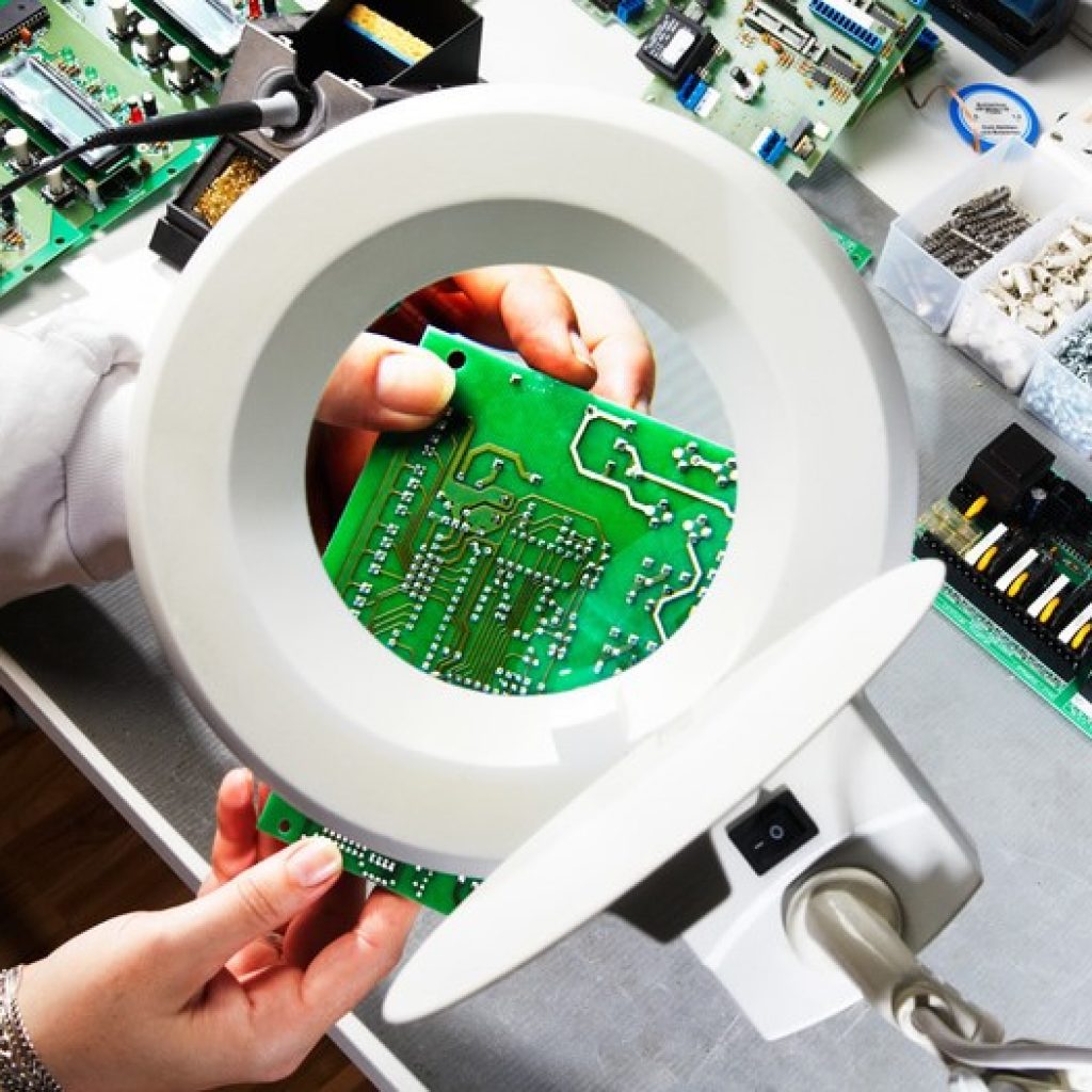
Ref: https://bayareacircuits.com/wp-content/uploads/2015/06/PCB-Inspection.jpg
Inspection after SMD placement brings up components that the pick-and-place machine has missed, wrong and imperfect component placement, and problems with solder paste depositions. Rush PCB uses high-power, multi-source, glare-free lighting to light up the PCB under inspection, and adjustable high-power lenses for the operator. These are essential for the operator to work without eye strain. Manual visual inspection methods are operator dependent, slow, and not suitable for high volume production.
Automated Optical Inspection (AOI): Instruments involved in AOI are high resolution video cameras connected to a computer, and adequate lighting. The computer uses algorithms to check the images of the PCB under test against an image of a good board stored in its memory, and highlights the differences.
Rush PCB uses high-power, multi-source, glare-free lighting to light up the PCB under inspection. AOI is high-speed and has the capability of inspecting many more assemblies without operator fatigue.
Inspections after the reflow stage highlights defects in soldering, such as dry solders, solder bridging, inadequate wetting, tombstoning, and others. Operators use the feedback from optical inspection to make finer adjustments to previous stages to ensure correction of defects.
X-Ray Inspection
Some fine-pitch IC packages such as BGA have pins arranged under them in the form of an array. This makes it impossible to inspect their connections optically after soldering. Rush PCB uses X-Rays to inspect the quality of soldering under the body of the package.
Technological Inspection
Rush PCB undertakes technological inspection after the reflow inspection stage to check for solderability and plating adhesion. For solderability, we inspect the wetting of solder to the conductive traces. For inspecting plating adhesion, we use qualified tips that we first stick to the plating under scrutiny, press evenly, and pull off quickly, while inspecting the plating for fall-off. We also check for copper foil peel-off and via metallization strength.
Electrical Performance Inspection
Rush PCB performs two types of electrical performance inspection—electrical conductivity and electrical insulation.
Electrical Conductivity Inspection: This is to inspect the conductivity of copper traces through metalized vias, mainly in double-sided and multi-layered boards. The focus of this test is on proper functioning of a metalized via connecting two or more traces on different layers. For this, the assembler selects strategic traces on the top and bottom layers of a PCB and measures the conductivity between them. A high resistance indicates a faulty via connecting the two traces.
Electrical Insulation Inspection: This inspection is to check for any accidental short between two independent traces on different layers of a double or multi-layered PCB. A low resistance indicates two traces, which should normally not have any interconnection, have an unwanted short joining them.
Read About: HOW TO CUT PCB ASSEMBLY COSTS?
In-Circuit and Functional Testing
In-Circuit Testing: This test requires a jig specifically made for a PCB assembly. The jig is usually in the form of several spring-loaded slim metal probes assembled in an array on an insulated bed. The assembly is also known as a bed-of-nails test jig. The testing professional identifies each probe by its X- and Y-coordinates. This test also requires the designer to place test pads at strategic locations on copper traces on the bottom layer of a double- or multi-layered board during PCB design.
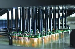
The testing professional places the assembled PCB on the probes and holds it down under pressure from the jig. This allows the probes to connect electrically to the test pads. The test involves checking various parameters such as resistance, capacitance, and inductance between specified probes, and highlighting the difference from an established chart of readings.
Functional Testing: This method allows testing the board assembly for its functionality and depends significantly on the PCB assembly under test. It requires connecting the PCB assembly to a specified power supply, apply requisite inputs, and check for specified outputs.
Functional testing of an assembled PCB requires information from the OEM to ascertain the outputs the test should produce.
Burn-in Testing
Rush PCB conducts burn-in testing to ensure the PCB assembly will perform as intended in real-life environments. The PCB assembly undergoes a specified time under elevated temperatures and after cooling down, should perform as intended under in-circuit and functional testing.
Read About: ADVANCED PCB MATERIALS AND GREENER MANUFACTURING
Comprehensive Inspection and Testing
Our comprehensive inspection and testing capabilities at Rush PCB allow us to meet all your requirements related to PCB assembly and production processes.
Please feel free to contact us via phone or email, or visit our website with your query.


