

Definition and Scope of DFA
As design decisions can have a significant effect on the cost and efficiency of PCBs during the assembly process, they can also affect the overall reliability and quality of the finished product. Design for assembly is a specific method by which design can take into consideration the cost and efficiency of the assembly process, as well as the functionality of the finished product.
In full turnkey services for PCBs, most of the cost relates to that of parts procurement and component placement. Therefore, a clear understanding of DFA principles can not only help to reduce the above costs, but also act in minimizing the overall lead time of the project, while protecting against assembly issues that necessitate time-consuming rework or even design revisions. As DFA principles relate closely to those of DFM (Design for Manufacturing), Rush PCB recommends considering both methods for creating the best possible product.
The scope of DFA guidelines mainly encompass understanding the capabilities of the assembly shop. This also affects the designers’ ability to achieve other strategies such as:
- Reducing components
- Combining components
- Using standard components
- Minimizing the risk
- Methods of simplification
- Achieving optimal clarity
- Understanding the capabilities of the assembly shop
Reducing Components
By reducing the total number of components necessary to mount on the board, not only will the total cost of the project come down, it will also reduce the total time taken by the pick-&-place machine to populate the board.
Of course, each design must meet a certain functionality and therefore, the presence of each component has its own justification. However, designs often contain extra features that OEMs may abandon in the pursuit of greater stability and better cost-effectiveness. By reducing the parts count, it is possible to reduce the Bill of Materials (BOM) of the project.
Combining Components
Component manufacturers offer many opportunities for combining components. For instance, they offer a single package for a combination of multiple resistors or capacitors required by low pass filters or in bus termination. Not only are these special packages cost-effective compared to the total cost of individual components, they reduce the time taken for reel changes and mounting at the assembly stage. When quoting for PCB assembly, Rush PCB takes into consideration the effect of reduction and combination, and passes on the benefits of cost and lead time reduction to the customer.
Using Standard Components
By using components that have performed well in the past, or those commonly available in the inventory, the designer can reduce the level of uncertainty that a new design brings.
By using stable and tested parts from earlier designs, the designer ensures not only the certainty of sourcing the component, but also the availability of the component with the same packaging. With our full turnkey solutions, Rush PCB offers the best combination of availability and reliability for components.
Minimizing the Risk
Although by reducing, combining, and using standard components designers can reduce some amount of risk involved with components, other aspects also need consideration, such as the fragility and weight of components.
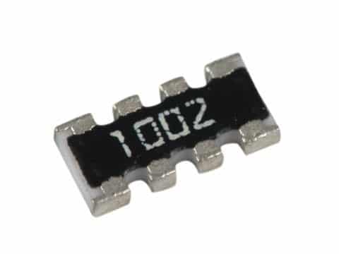
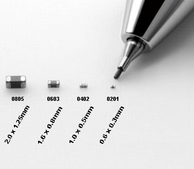
Fragility of a component can drastically affect the assembly times. By reducing the potential complications during assembly such as component breakages or loss, designers can increase the efficiency of the assembly line. For instance, use of 0201 SMD size of components increases the likelihood of missing components, resulting in additional assembly time and cost to compensate for the numbers lost in production and the necessity for maintaining additional stock. Rush PCB recommends the use of 0603 SMD size instead, provided there is available space.
Mounting heavy and unwieldy components on the PCB can also add to handling and shipping costs. While Rush PCB recommends eliminating such parts from the PCB, it may not always be possible for the designer. The efficiency of the assembly line depends on several factors, such as whether the heavy part requires manual assembly, if it is a through-hole part, or if the final assembly requires additional attention. All the above add to the cost and lead time of the PCB assembly.
Methods of Simplification
While minimizing the risk is one form of simplification, other complications can arise from complex parts and complex process requirements. Simplifying these complications can improve the efficiency of the assembly line. In a PCB project, although it may not be possible to avoid risks entirely, it may be feasible to simplify or even eliminate complications by innovative design techniques.
In modern PCB design it may not always be possible to exclude complex parts such as POP, Flip-chips, CSP, QFN, LGA, or BGA packages. Additionally, these extraordinary packages also require special design techniques such as via-in-pad and dog-bone style fan-out for routing traces.
Achieving Optimal Clarity
The PCB assembly process can proceed with utmost efficiency only if all documentation is clear and consistent. Lead times can increase when Rush PCB must solve complications arising from information in one document disagreeing with that in another—for instance, when design revision in one document does not reflect equally in another.
CAD programs often automatically generate the BOM for a project. Rush PCB recommends a manual review of the software generate BOM for inconsistencies, incompleteness, ambiguity, missing or inaccurate parts, mismatch between description and part number, and mismatch between reference designator and quantity.
Rush PCB recommends clarity in the file providing XY coordinates for the pick-&-place machines, as we use this information to directly program our pick-&-place machines for automatic parts placement. Although CAD generated, chances of error are always present, especially with incomplete project updates, in the form of missing parts, and inaccurate coordinates.
The rest of the Gerber files also require clarity. For instance, the legend printing layer or the silkscreen layer may have markings for polarized components inconsistent with the actual layout, mainly as a result of incomplete project updates.
Understanding the Capabilities of the Assembly Shop
When understanding the capabilities of the assembly shop, the following areas need special consideration related to components:
- Orientation
- Sizing
- Spacing
- Standards
- Reflow Soldering
- Wave Soldering
- Manual Soldering
- Special Requirements
- Typical Assembly Issues
- Testing Methods
Component Orientation: The designer must specify this parameter in the assembly drawing and it must correspond to the Gerber files. Rush PCB recommends following IPC 7351B or later standards for depicting component orientation.
Component Sizing: Although Rush PCB can handle SMD packages down to 0201 for resistors and capacitors, we recommend designers use larger sizes for DFA purposes, unless the design specifically demands such small components. Rush PCB also recommends not placing large SMD packages such as QFN, QFO, or BGA in the center of a PCB, as this is where the maximum camber, bow, and twist is likely to occur.
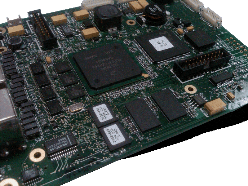
Moreover, to ease X-ray inspection, Rush PCB recommends not placing large packages on top of each other on both sides of the PCB, rather placing them only on one side.
Component Spacing: The land pattern design of each component and spacing between neighboring parts must be adequate to protect against potential faults such as solder bridging. Although larger spacing between parts does offer better quality of PCB assembly, Rush PCB recognizes the requirement of tight spacing for OEMs to achieve small form factors.
Other important factors to look for during the DFA session relate to:
- Part-to-Edge Spacing
- Part-to-Hole Spacing
- Part-to-Annular Ring Spacing
- Pad and Hole Sizes
- SMT Pad-to-Lead Aspect Ratio
- THT Hole-to-Lead Aspect Ratio
Quality Standards: Rush PCB handles several unique and specific PCB assembly requirements, and recommends customers to specify certain industry standards they want their PCBs to comply with, such as IPC, SMTA, and ISO. Specifying these standards makes it easier for Rush PCB to offer assurances that PCBs will meet or exceed the requirements.
Reflow Soldering: Although Rush PCB recommends complete reflow solderability for PCBs as this offers the best efficiency, we can handle manual and wave soldering as well. Major considerations for the designer should be to use components capable of withstanding the high temperatures associated with Lead-free soldering. Designers must match the heat tolerance level of each component specified by the manufacturer to the heat requirement for a standard reflow cycle.
Wave Soldering: If the board has several through-hole components, Rush PCB recommends wave soldering for better assembly efficiency. However, wave soldering requirements have stricter controls in design and the designer must address them.
Manual Soldering: For mounting parts that are not suitable for either reflow or wave soldering, Rush PCB offers manual soldering by a staff of highly skilled manual soldering specialists. However, the designer must understand and address the restrictions manual soldering entails.
Special Requirements: Rush PCB can also handle special requirements in assembly, such as adhesive application, conformal coatings, heat sinks, and EMI/EMC shields. For implementation, designers must include detailed drawings with measurements for clarity. DFA reviews must evaluate special requirements on case-to-case basis.
Typical Assembly Issues: Although Rush PCB employs several quality control methods during PCB fabrication and assembly to avoid defects, designers can also contribute to avoiding them by focusing on them during design. For instance, designers can avoid tombstones during reflow soldering by ensuring both pads of an SMD component are of the same dimensions, and that more than 50% of the leads contact each pad. Other typical assembly issues that designers can control are creation of tin whiskers, solder bridges, solder balls, and joint voids.
Testing Methods: One of the subsections in DFA includes Design for Testing (DFT). The OEM must clearly define the type of testing they require for their PCB project. Rush PCB can handle different types of testing, including Automated Optical Inspection, X-ray Inspection, and Functional Circuit Testing (FCT).
Conclusion
Rush PCB recommends considering DFA principles for creating high-quality PCBs most efficiently, and at the lowest possible cost. The above guideline should give our customers a clear idea of DFA requirements and the possible benefits to them during PCB assembly. For any questions not answered by the guidelines, please call Rush PCB through live chat or contact over email.


