

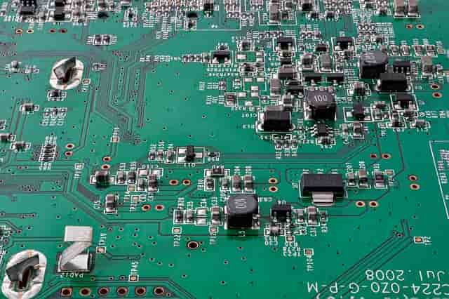
A printed circuit board or PCB is an essential part of any electronic equipment. It is a special component that holds together various electronic and non-electronic components on itself, allowing them to work harmoniously. According to Rush PCB USA, the constituents of a PCB include an important layer known as the silkscreen, and it offers vital printed information.
The silkscreen layer on any PCB tells the assembler where on the board they must place which component, and in what orientation. Typically, the silkscreen has a unique designation for each component, and the assembler can refer this designation in the Bill of Materials to know all details about the component.
What is a Silkscreen?
The designer creates the silkscreen as a layer and adds it to the other layers of a PCB. The fabricator will apply the silkscreen to the PCB only if the designer has requested for it in the special instructions. The designer includes various information on the silkscreen layer like:
- Reference designators for all components on the board
- Orientation of the components
- Polarity of the components
- Outline of the components
- Test Points
- Warning symbols
- PCB version number
- PCB serial number
- Manufacturer’s logo
- Testing certifications
For a PCB with SMCs or surface mount components only, the designer may use only one silkscreen layer meant for the top upper surface of the board. When the PCB has through hole components or THCs, the designer may divide the silkscreen into two parts. The silkscreen for the top upper surface has most of the information, while the silkscreen for the bottom surface additionally shows the reference designation, orientation, and polarity of the components. For the printing on the PCB, fabricators use non-conductive epoxy ink. The designer must ensure that the printing ink of the silkscreen does not intrude on the copper pads meant for soldering.
Methods of Applying the Silkscreen
The fabricator uses the silkscreen information to make a transfer screen when they want to manually transfer the information on the PCB. However, they may also use newer methods of directly printing the information on the PCB. In the second case, no transfer screen is necessary.
Manual Printing of the Silkscreen
The manual method of printing the silkscreen is helpful as long as the line widths are more than 0.007 inches or 7 mil and the registration tolerance is not lower than 0.005 inches or 5 mil. The fabricator uses the text and trace information in the silkscreen layer to generate a stencil on a nylon fabric. This fabric is stretched on a frame, allowing epoxy ink to pass through the stencil and creating the silkscreen print on to the surface of the board. The board requires curing in an oven to fix the ink on the PCB surface.
For a better understanding of the process watch https://www.youtube.com/watch?v=tth9xdEIwiQ
Liquid Photo Imaging of Silkscreen
For thinner line widths such as 4 mil, manual printing is not suitable and fabricators use the liquid photo imaging or LPI method. They coat the PCB with a layer of light sensitive epoxy. They impose the image of the silkscreen on the epoxy and expose it to UV light. They chemically remove the unexposed part of the epoxy, leaving the image of the silkscreen on the board, which then undergoes fixing by curing.
Although the LPI method offers higher accuracy compared to the manual printing method, it uses more ink and requires more setup time.
Direct Legend Printing of Silkscreen
This method is the most accurate and also most expensive of all others. It requires a computer, CAD software, acrylic ink, and inkjet projector. The computer directs the projector to inject ink on the PCB according to the silkscreen print, which them undergoes UV curing.
To better understand the process watch https://www.youtube.com/watch?v=mwy9Kigv9Mg
Why Use Silkscreen Print on a PCB?
There are several benefits of using a silkscreen print on a PCB. For instance, with the silkscreen print:
- Assemblers can use the reference designators to accurately position components on the board.
- Assemblers can identify the orientation and polarity of the components.
- Technicians can identify the test points on a PCB when troubleshooting or taking measurements.
- Technicians can see the warning symbols for high voltage, and set specific voltage and current levels accordingly.
- Technicians can easily identify components they must replace when repairing the board.
How to Design a Silkscreen for a PCB?
To improve the quality of the PCB component identification, assembly and testing, it is necessary the silkscreen meets certain design specifications. According to Rush PCB USA, these include:
Fonts — Not all fonts are suitable for silkscreen printing on the PCB. The designer must consult their contract manufacturer for the fonts that will be legible and readable after printing.
Color — As the fabricator applies the silkscreen over the solder mask layer, the color of the ink for the silkscreen should provide a contrast over that of the solder mask. White silkscreen color works best on a green solder mask layer, but any contrasting color that allows easy readability should be acceptable.
Clearance and Dimension — For proper legibility and readability, the lines and letters of the silkscreen must have proper clearance and dimensions. The designer must consult their contract manufacturer on this aspect. In no case must the ink from the silkscreen printing intrude upon the solderable copper pads.
PCB Design Guidelines and DFM — The above information should be part of the PCB design guideline and Design for Manufacturing or DFM. This will ensure all silkscreen for different PCBs will have a standardized design.
Conclusion
According to Rush PCB USA, using a silkscreen print on a PCB helps to improve its quality and reliability substantially. This is because a silkscreen helps in the assembly and testing stages, while simultaneously reducing troubleshooting time substantially. The extra cost of including a silkscreen layer print is definitely worth the improvement in the PCB quality and reliability.


