

Rush PCB makes two types of Printed Circuit Boards (PCBs), one with non-metalized edges and the other with metallized edges. Earlier there was not much demand for metal-edged PCBs, but now more customers are demanding it. There is greater attention for higher quality of PCB metal edging as it enhances the functioning of several products that use these PCBs. The industry has many names for a PCB with metallized edges. Some of these names are side plating, plated contour, border plating, edge plating, castellation, etc.
Why Metal Edging on PCBs
With miniaturization and increasing high-speed operation of circuits, the timing of the digital signals and their signal integrity are prominent issues. Additionally, medium-high-speed digital signals in the system can generate Electro-Magnetic-Interference or EMI and Electro-Magnetic-Compatibility or EMC issues because of power integrity. EMI from high-speed digital signals can create serious interference not only within the system but also radiate them outside the system, making the device exceed the safe limit standards of EMC. One of the common sources of EMI is the unwanted radiation from the sides of a multi-layered board.
Power and ground planes carrying current generate electromagnetic radiation at their edges. Most of the noise comes from stray currents in power and ground planes because of insufficient power supply bypassing. At high-frequencies, a through-hole via acts as a stub and can have high inductance. Such a via can radiate magnetic fields between various layers of the board, ultimately gathering them at its edge.
The board metallization edging process from Rush PCB encloses the entire board edge with a metal. This short circuits the high-frequency signals that arrive at the board edge, preventing them from radiating. Although this improves the board performance, the process of edge metallization increases the cost of the PCB.
PCB Edge-Plating Process
Fabricating circuit boards for edge plating requires careful handling of the board. The manner of preparation of plated edges generates many challenges, one of them being assuring the adhesion of the plated material to the board for its lifetime.
Rush PCB uses industry established practices including several optimized standards for ensuring the castellation of PCB edges will prepare them thoroughly while applying plating copper for contiguous adhesion. We process the board to ensure each layer adheres for the entire life of the board.
Our circuit board fabrication uses a controlled process for edge metallization. This allows us to plate all the through-holes and half-holes on the edge of the PCB. We take special care to prevent creation of burrs, and these can lead to failure of the edge metallization process.
We ensure that internal power planes never approach the edge of the board for the board metallization edge process, as the edge plating can cause them to short electrically. In our DFM studies of a PCB that requires edge plating, we always ensure there is a gap between the edges of power planes and the edges of the board.
The PCB edge-plating process is the same as for plating through holes. However, the board must fulfill two requirements for an edge plating process. The first is, the board edges must undergo proper milling or scoring to ensure they are smooth and without burrs. The second is, the top and bottom layers must include an anchor copper strip around the edges of the board. In case the board is a part of a panel, the edge-plating will not cover the entire length of the edges. The plating process will exclude the part of the edge connecting the board to the panel.
The drilled board undergoes a thorough cleaning process and then passes through a series of chemical baths. The process deposits a thin layer of copper over the outer surfaces of the board. This thin layer of copper covers the sides of all the through holes including the castellation holes, and joins the copper track on the top layer edge to the copper track on the edge of the bottom layer across the side of the board.
Designing PCBs for Edge-Plating Process
To ensure the manufacturability of edge plating, Rush PCB defines the metallized area with overlapping copper such as copper surface, traces, or pads in the layout files. Some thumb rules we follow are:
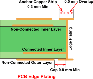
Overlap — a minimum of 0.5 mm
Connected Layers — define connected copper with 0.3 mm minimum width
Non-Connected Layers — minimum of 0.8 mm gap from outer contour.
While defining edge-plating for manufacturing, Rush PCB makes sure of adding manufacturing notes on fab drawings pointing to the relevant edges:
- Edge-plating area: use X Oz copper, break any sharp edges, and deburr.
- XXX plane on layer(s) N (and N) connect to the edge-plating area.
Benefits of Edge-Plating
With edge-plating, Rush PCB offers printed boards of higher quality and reliability. Benefits of edge-plating include:
- Better protection to edges
- Edge connections with improved reliability
- Extra copper adds to PCB’s ability to carry current
- Improved thermal distribution. Internal layers connected to edge-plating can distribute their heat to the plating for dissipation to the surrounding air. This improves the reliability of the board.
- Improved signal integrity. The presence of copper on the edges of the board prevents external interference to internal signals.
- Improved EMI/EMC performance. Allowing stray return currents to shunt through the edge-plated copper prevents the generation of sporadic magnetic and electric fields.
Conclusion
Rush PCB offers edge-plating as a great way for ensuring a strong connection and reducing the chances of expensive board failures. We offer edge-plating with surface finishes in HASL, ENIG, ENEPIG, and others. The industry uses side-plating as a feature for later PCB assembly.


