

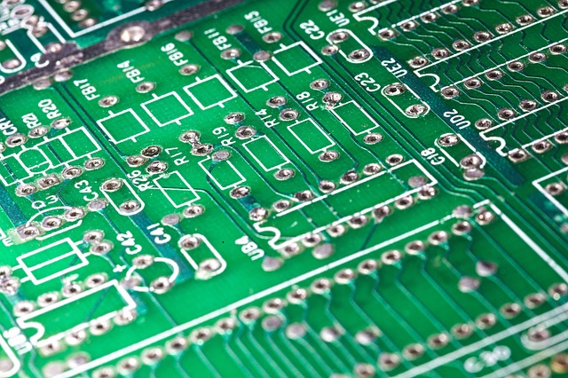
At Rush PCB Inc, we manufacture various types of printed circuit boards or PCBs. During manufacturing, we must pay a lot of attention on handling different tools and processes to avoid common quality issues. These issues include cold joints, brittle joints, and voids. A void is an empty space somewhere in the PCB that has an inadequate amount of material. The voiding issue is important enough, and if not addressed properly, may lead to scrapping the PCB.
Therefore, it is necessary to understand the issue with voids and the additional problems voids create. The PCB manufacturing process has mainly two common types of voids, and it is imperative for our customers to know the measures we take to avoid them.
PCB Voids
Voids in a PCB can occur anywhere in its non-plated areas. This can be either within the wall of a drilled hole under the plating, within the barrel of a hole, or within a solder joint. Voids tend to disrupt the electrical continuity within the circuit, leading to the PCB malfunctioning. PCB voids are mainly of two types:
Plating Voids
During the electroless copper plating process, the plating may not completely cover the inner walls of a PCB hole, thereby creating a plating void. Such voids typically occur due to the drilling process when creating a through-hole. If the drill bit is dull, it does not create a smooth wall surface when drilling, but will leave imperfections along the wall.
The hole wall formed by a dull drill bit is usually rough with many imperfections. When adding copper during the electroless copper plating process, the copper may not enter into all the rough dips and crevices in the hole wall, and this leaves many non-plated spots.
The drilling process may also cause debris to lodge inside the hole. Typically, such debris may be the result of a worker removing the drill bit, and not cleaning the hole adequately. When plating a hole with a debris or other contaminant lodged inside, the copper plating may temporarily cover the debris or contaminant. Subsequently, when the debris dislodges from the hole wall, it might as well remove the copper covering it, thereby leaving a void.
Another way a plating void forms is when the hole wall has an entrapped air bubble on it. The bubble prevents copper deposition under it during the plating process, thereby creating a void.
Preventing Plating Voids
Using sharp drill bits is one way to prevent voids that the drilling process creates. Operators must discard or sharpen drill bits based on drill speeds, feeds, and hit count records. They must follow each drill hole with a cleaning procedure and proper racking. Monitoring the plating bath agitation in the tanks can also help to reduce and eliminate plating voids. For instance, use of line vibration and angled plating racks can release entrapped air during the electroless plating process. We avoid using drill bits after a certain number of hits, and we never reuse drill bits. Additionally, we perform a desmear process to remove foreign particles that are generated during drilling
Solder Voids
Solder voids happen when the operator uses inadequate amount of solder paste. Additionally, the solder paste may have air pockets, which did not escape when the solder paste underwent inadequate heating. Both cases of void formation can lead to the board becoming inoperable and the manufacturer may have to scrap it.
Empty spaces inside a solder joint may also generate a solder void. Many factors may lead to this issue, including a low preheat temperature setting, as it prevents the solvent within the flux from completely vaporizing. Other factors include high levels of flux, oxidization of the solder paste, or the use of low-quality solder paste. In some cases, the design of the PCB, and its stencil, may also make it more prone to voiding. Typical causes of solder voids are:
- Inadequate preheat temperature during reflow
- Outgassing of organic brighteners
- Impure or low-quality flux in the solder paste
- Presence of water/humidity on the PCB surface or in the solder paste
- Excess oxides on silver deposits
- Contamination of solder mask on the copper
Preventing Solder Voids
Among the two main types of voids, it is typically much easier to prevent solder voids than it is to prevent plating voids. Effective ways of mitigating the risk of solder voids include modifying the stencil design, avoiding the use of outdated and/or low-quality solder paste, and simply extending the preheat time.
Micro Voids
Micro voids are another type of solder voids where numerous small voids form at the interface of a solder joint. Micro voids are typically less than 40 microns in diameter, and appear just above the intermetallic junction layer between the copper on the circuit board and the tin from the solder paste.
As with solder voids, micro voids can be troublesome when existing in sufficient numbers and reducing he cross-sectional area of the joint. In extreme cases, the presence of many thousands of micro voids can make the joint fail electrically and physically. Earlier, there was no way to detect the presence of micro voids. Nowadays, it is possible to use high-resolution X-ray inspection methods to detect the presence of micro voids.
The growing use of lead-free solder is one of the reasons for an increase in micro voids. The lead-free solder reflow process needs higher temperatures as compared to leaded solders. This increases the possibilities of temperature variation across the board. Moreover, differences in flux chemistry and surface tension between brands of lead-free solders may also be the cause of micro void formation.
Coupled with the transition to lead-free solder, manufacturers also offer new surface finishes for PCB boards. For instance, immersion silver is a popular surface finish. However, process control issues such as contamination of the board surface due to oils, developer foam, tin resist, and films of sublimated solder mask volatiles, may also lead to formation of mico voids.
Another reason for the formation of micro voids is the inordinately rough surface on the copper pads. Just as solder joints may have several micro voids leading to a large solder void, small pockets of entrapped air on the rough copper surface can create micro voids.
Several processes can cause the copper surface to roughen. Variations in current density during the plating process can produce a rough surface by varying the deposition. Solder mask preparation or tin stripping can also affect the copper surface adversely prior to surface finish. Although the surface finish process uses a micro-etching and cleaner agents, these are relatively mild substances, and therefore, cannot overcome filthy or rough copper surfaces.
Reworking the silver finish can also affect the copper surface adversely. This happens when operators repeatedly rework the silver finish by processing the PC multiple times through the plating bath. This impacts the integrity of both the silver deposits and the copper surface.
Preventing Micro Voids
Although very high thicknesses of silver finish does cause micro voids, it is not possible to drastically reduce the thickness of immersion silver finish. For instance, a plating thickness below 0.13 micron will lead to increased migration of copper through pores, increased tarnishing, and possible loss in contact function. By keeping the thickness of immersion silver finish above the lower limit, it is possible to reduce formation of micro voids by reducing the silver thickness.
However, keeping tabs on the quality of immersion silver does not amount to much if other processes are not maintained and engineered. The copper surface must be free of tin and organic residues. The roughness of the copper surface must be fairly low. The micro-etching process prior to silver deposition must produce copper with a uniform, clean surface.
There must be a restriction on rework based on supplier recommendations. Multiple rework can generate rough silver surface that perform the same way as thick silver deposits do. After silver deposition, it is necessary to control the ionic residue on the board by rinsing, and handling and packaging with care.
During assembly, it is possible to prevent the formation of micro voids by using a medium preheat temperature and low ramp rate. Additionally, it may be necessary to use low-voiding fluxes and exercise better control over storage of solder paste for effectively preventing micro voids.
Conclusion
PCB scrapping due to voids can very quickly make the manufacturing of PCBs an expensive process. According to Rush PCB Inc, some amount of precaution and extra attention to details is enough to prevent the formation of PCB voids. It requires using good quality sharp drill bits, better cleaning procedures, and extensive testing to reduce void formation and ensure high quality of boards.


