

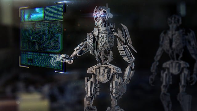
Artificial Intelligence or AI has been making inroads into our technological world over the last one decade. AI is a forward-looking and futuristic concept, and nearly all industries are using it widely for a vast array of applications. As a result, we now have Alexa, Siri, and many other AI-driven voice assistants, self-driving cars, Internet search engines, and many others. The use of AI is widely spreading and growing exponentially.
According to Rush PCB Inc, there are two primary ways PCBs or printed circuit boards influence AI applications and vice versa:
PCBs for Devices using AI
The trend in the electronics industry is towards making devices smarter. Embedding AI in robots, voice assistants, and autonomous vehicles helps achieve this superbly by using advanced microcontrollers and other electronic components. All electronic devices need a printed circuit board to function, and devices using AI are no exception. However, the introduction of AI in devices being a futuristic concept, the process opens up new challenges in PCB design and manufacturing.
AI Influencing PCB Design and Manufacturing
Just as smart devices using AI need PCBs to make them functional, PCB designers and manufacturers are also utilizing AI. Artificial Intelligence is assisting them in opening up newer and more efficient methods of PCB fabrication, optimizing the costs, reducing scrap and turn-around times, and improving the utilization of supply chains, inventory, and assets.
AI helps in two ways—it helps systems communicate with each other, and it helps systems communicate with operators. For instance, during PCB assembly, AI helps in determining the precise placement of SMD components. This not only reduces the assembly time, it also improves the quality of the board significantly. With the trend in the electronics industry moving rapidly towards form-factor miniaturization, fast and accurate placement of components prior to soldering is a huge advantage.
Use of Printed Circuit Boards for AI Applications
All electronic devices, whether using AI or not, require printed circuit boards for functioning. Implementing AI in devices requires additionally incorporating special miniature components, typically like SoC, flip-chips, and micro BGA using fine-pitch packages.
PCB manufacturers achieve this by fabricating boards with a special technology known as HDI or High Density Interconnect. HDI allows achievement of very high component densities by using thin, closely packed traces and very small vias or microvias.
Advantages of HDI Technology
HDI technology is the leading contributor to performance improvements required in PCBs for devices in AI applications. Not only does HDI make the PCB smaller, lighter, and thinner, it improves the electrical performance. Some advantages of using HDI technology are:
- Very low electrical parasitics — Low EMI, high-speed operation, better signal integrity
- Minimal Stubs — Low signal reflection
- Stable Voltages — Lower track resistance
- Decoupling Capacitors not Required — Due to low electrical parasitics
- Lower Noise and Crosstalk — Due to better signal integrity
- Lower EMI and RFI — Due to microvias, via-in-pads and surface ground planes
- Closer Ground Planes
- Better Distributed Capacitance
Advantages in using HDI technology are further supported by semiconductor manufacturers offering components with reduced sizes. The smaller overall size of the board and components allows faster rise and fall times for signals. This manifests itself as better high-frequency operation.
However, smaller component sizes means there is less surface area for heat dissipation. HDI, therefore, calls for better thermal management. PCB manufacturers achieve this by using high-performance laminates. Apart from better thermal management, high-performance laminates also help in improving signal integrity. Use of stacked microvias also helps in improving high-speed performance of HDI boards.
Laser-drilled microvias are nearly one-tenth the size of mechanically-drilled through holes. Therefore, microvias offer the advantage of lower parasitics and lower inductance, while improving the high-speed performance. Via-in-pad design also helps further in noise reduction and high-speed operation.
AI offers a significant advantage during inspection of boards. The AI logic is very efficient for discovering defects like wrong components, missing components, misplaced components, and track defects. This is especially helpful when using tightly-packed miniscule components on HDI boards.
AI Enhancement of PCBs
PCBs being the platform using which miniscule electronic components and systems interact mutually, its design and manufacturing process significantly influences electronic devices. PCB manufacturers, therefore, take help of AI induced enhancements for design and quality of their boards. To this end, FIT or the Fraunhofer Institute of Applied Information Technology offers a modular AI platform that helps in optimizing the design and testing of PCBs. The platform comprises modules for machine learning, deep learning, and artificial intelligence. Using this platform, it is possible to reduce the outlay for PCBs by as much as 20%.
Each module in the platform uses algorithms trained for different tasks. For instance, an algorithm in the first module helps in classifying input data, extracting features from the data, and providing the input that other modules will need.
When designing a new PCB for an application, the designer takes care to make the best possible use of the available space, while packing the components as close together as possible, without risking failures. The present design process largely relies on the experience of engineers, and the design must undergo tests in real trials. Most often, it is easy to overlook documentation of test results, leading to repeat testing of the error-prone design, further increasing costs.
Quality Assurance Demands High Outlay
The complex design of PCBs requires manufacturing processes to follow exacting specifications. To achieve this, each PCB undergoes stringent tests on completion. Typically, one such test is the automated optical inspection or AOI.
AOI uses image analysis techniques to determine if the PCB manufactured conforms to the design specifications and is free from technical defects. The present methods in use, however, produce a high false negative rate, incorrectly classifying many boards as defective.
These wrongly classified boards then require another level of manual or machine inspection. Therefore, a high false negative rate wrongly rejects non-defective PCBs, which then require reinspection, resulting in adding to the cost. On the other hand, a low false negative rate can mean high follow-up costs, as many defective boards enter the workflow. All this means it is very difficult to achieve an ideal positive or false negative rate depending on present AOI and human inspection methods.
Self-Learning Techniques for Optimal Selection
FIT demonstrates what AI can do during a future inspection process. The process remains the same as in the conventional AOI, that is, a camera captures images of the PCB. In this case, however, it is vital that the images are of a high-quality, as these will be the training data for the AI modules. It is imperative that only a good selection of images reach the modules for machine learning and deep learning.
According to the project manager at Fraunhofer FIT, the modular design has several algorithms that enhance their own performance continually. Ongoing automated inspection of boards continuously feeds back the generated data to the algorithm. This forms a self-learning process for the AI module. The feedback enhances the database, while optimizing the true negative rate. Actual industrial experience with this module indicates a 20 percent reduction in the use of production resources.
Intelligent PCB Design and Fabrication
After completing the training, the AI module can also help to design new PCBs. This helps in cutting down the time required for arranging components on board using the trial and error method presently followed by designers for obtaining an optimal configuration. Rather, the AI module algorithm helps to predict the most optimum configuration to achieve the best functionality.
PCB design is only one instance of where a self-enhancing AI module can help to enhance the quality assurance. This self-learning AI module is equally effective in other areas of the PCB manufacturing process, such as in optimizing the etching process, the reflow process, and other time intensive activities to achieve significant savings in time and production costs.
Deep Learning and Machine Learning
Many industries, including PCB manufacturing, are reaping the benefits of deep learning and machine learning through artificial intelligence. Essentially, it requires the effective use of data for gaining experience for solving complex problems with near-zero intervention from humans. Machine and deep learning, when applied to the PCB design and manufacturing processes, can go a long way in improving not only the operation, but also in reducing the cost of human intervention.
Conclusion
According to Rush PCB Inc, the positive impact of AI in PCB manufacturing is invaluable. However, the industry must meticulously develop the above factors for completely harnessing the huge potential of AI. This requires dedicating enough time and resources to the usage of AI in the PCB manufacturing process. Ultimately, this can lead to an era where the production process is fully streamlined with an exponential improvement of outcomes.


