

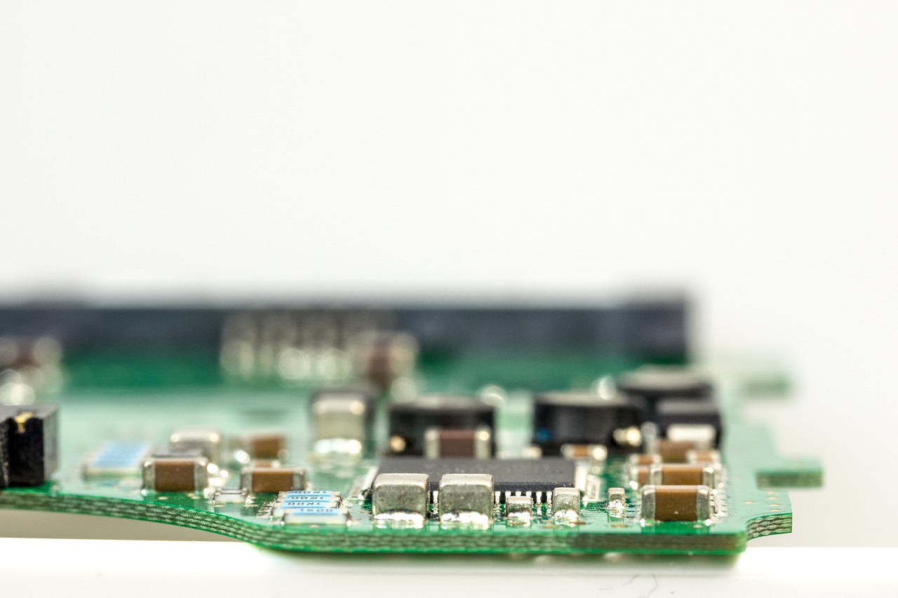
Almost every electronic item around you consists of one or more Printed Circuit Boards (PCBs). PCBs hold components and also provide connections between these components.
So, if you’re an Electrical or Electronics engineer, the chances are that you will design PCBs at some stage in your career. Despite this design being a key function of electrical engineering, it’s not something that is widely taught in engineering programs. It’s not difficult for engineers to understand the core functions required for effective PCB design. There are a lot of elements to consider. All functional requirements must be met including schematic designs, component placement, and routing. Other factors that need to be considered include the schedule and cost.
Create a Schematic Diagram
Converting the concept of requirements into a PCB will require electronic language and logic. Start with a schematic diagram. The schematic diagram will include the overall design and the interconnections between circuits and components, identify the component placement, and address other factors such as the PCB material and temperature requirements.
Generate a Bill of Materials
The Bill of Materials (BOM) should be generated in conjunction with the schematic diagram. It is a summary of all the components and links required for production of the PCB. There are five key aspects of the BOM:
- The number and type of each component.
- The identification of a component in a circuit on a PCB.
- The numeric value of ohms, farads, etc.
- The footprint of each component on the PCB, and if available
- The manufacturer’s part number.
Placement on the PCB
Each component will need to be located based on function, thermal management and electronic noise. The order of placement is:
- Connectors,
- Power circuits,
- Sensitive and precision circuits,
- Critical circuit components,
- Everything else.
Following the initial placement, the PCB should be tested and reviewed, with adjustments made based on power tolerance and budget.
Routing
All PCB components are interconnected through routed traces. Elements that should be considered in routing include power levels, noise sensitivity (or generation) and routing capability. As a guide, traces with a width of 10 to 20mils can carry the current of 10 to 20mA and 5 to 8mils of carrying current lower than 10mA. If there is a requirement for high-frequency or rapidly changing signals, designers should consider routing using high-frequency nodes.
Thermal Management
Heat is a crucial factor in design. An ideal design will keep the entire board at a uniform temperature during operation. The components and links with different thermal activity need to be balanced in the design. Factors to consider include copper thickness, the number of layers and the board size.
Three ways of addressing heat include ensuring solid ground or power planes with more layers that are connected directly to heat sources; ensuring the heat transfer is optimized by developing effective heat and high-current routes; and by maximizing the area used for heat transfer.
Completing a Final Check
A final check of the design will include Design Rule Checking (DRC). DRC will determine whether the physical layout of the PCB meets Design Rules (a series of recommended parameters). This is a major step during signoff on the design, and includes validating Layout Versus Schematic (LVS), XOR, Electrical Rule Checks (ERC) and Antenna Checks.


