

All printed circuit boards (PCBs) use copper as traces in the core and all the layers. Even the outermost layers contain copper as the main component. According to Rush PCB USA, inconsistent distribution of copper in the layer stack-up can lead to many issues like bow, twist, and warpage.
Bow
PCBs can acquire a spherical or cylindrical curvature due to inconsistencies in copper coverage. A PCB with a bow undergoes compression or tension on its surface depending on the direction of the bend. Depending on the extent of the bend, the board may have unequal circulation of current across it, increased EMI/EMC effects, and lower reliability.
Twist
Ideally, all corners of a PCB are in the same plane. Inconsistency in copper distribution may twist the PCB such that two of its diagonally opposite corners lift upwards, while the other two corners move downwards. A twist in the PCB board causes stress in all its layers.
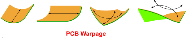
Warpage
Inconsistency in copper distribution may lead to warpage or bow and twist of various types in PCBs. This is also known as the potato chip effect. Not only can warpage cause non-uniform distribution of current across the board, it may also lead to cracks in traces and leads of mounted components, causing interruption of current and major disruption in the functioning of the board.
What Causes PCB Warpage
During manufacture and assembly, a circuit board undergoes many stages of heating and cooling. These may happen during pressing, etching, electroplating, application of solder mask, and during soldering of components. In each of these processes, copper in each layer and the substrate material expand and contract at different rates.
The substrate material is mostly consistent throughout the layers of the PCB, whereas the copper distribution may not be equally consistent. With the two materials expanding and contracting at different rates, the PCB may undergo distortions. Repeated distortions can result in the board taking up a permanent warped shape.
Even Copper Distribution Prevents PCB Warpage
Although fabricators manufacture PCBs in accordance with international standards like IPC 600A (Rev.G), several factors contribute to PCB warpage, bow, and twist. To some extent, there is contribution from type of surface finish, substrate material, etc., but the major contribution is from inconsistent copper distribution.
Observing some basic rules during the layout phase can help in reducing or even preventing PCB warpage later. Designers must ensure they distribute the conductor traces uniformly across the layer, thus avoiding the creation of copper nests.
Designers must follow the same consideration across an axis of symmetry between two or more layers. For instance, if a layer requires massive copper fills, the symmetrically opposite layer must also have a similar copper filling to counterbalance the former. Filling the open areas with copper in both layers is necessary to form a counterbalance.
Apart from similar copper filings in symmetrical layers, the planarity and thickness of copper in these layers is also important. Therefore, even distribution is important not only on the surface, but in the volume of copper also. This is because an uneven distribution of copper on the layers of a multilayer PCB, a non-symmetrical distribution, or an uneven thickness of copper above and below the horizontal center of the board may lead to an imbalance in its mechanical stability.
Uneven Copper Distribution Affects Vias
An even copper distribution results in higher mechanical stability, with reduced chances of the board distorting during the manufacturing and assembly processes. Moreover, an evenly distributed copper is also helpful in the electroplating process, as it results in a uniform thickness of plating, not only on the copper track surface but also on the barrels of plated through holes.
Uneven Copper Distribution Affects dielectric Thickness
An even distribution of copper allows more accurate control of the dielectric thickness between copper layers. Fabricators use prepreg as the glue to bond layers together. This is a flexible fiberglass-based material impregnated with a semi-cured epoxy resin.
As the fabricator stacks the layers, they place sheets of prepreg between them. When the layers are put under press and heated, the prepreg liquifies and flows to fill in the gaps between the copper features, ensuring air is not trapped inside the board. Any trapped air would heat up during assembly, and start outgassing. This could lead to a delamination of the board or ejecting components off the board.
An even distribution of copper ensures control over the amount of prepreg to use, resulting in consistent dielectric thickness.
Ensuring Even Copper Distribution in PCBs
Designers can use the free tool, PCB Visualizer, available online, to verify if the copper distribution in their PCB will result in a uniform plated surface. The tool uses the copper distribution and density to calculates the plating index on the outer layers. If the plating index is low, it indicates there is large variation in the copper thickness.
The tool divides the PCB surface into cells. It calculates the copper density of each cell, and compares it to the average copper density of the entire board. Based on this information, it assigns a color to each cell. Cells that it marks in blue run the risk of being under-plated, while those it marks in red indicate they are at risk of being over-plated.
A plating index of 1 indicates the electroplating process will provide an even plating throughout. A value of less than 1 indicates there is going to be non-uniformity in copper plating, with red and green areas as the highlight zones. A plating index lower than 0.4 is indicative of manufacturing problems, affecting the reliability and quality of the board, while increasing scrap.
The manufacturing process of a PCB unavoidably leads to changes in copper thickness over the board. This is because the galvanic process does not result in even building of the metal lattices of copper. Moreover, almost every manufacturing step has a cleaning process after it, resulting in removal of small amounts of copper. Furthermore, manufacturers start with a base copper thickness that has a tolerance of about 10%.
Adding Copper Thieving
Manufacturers frequently add copper thieving to a PCB. They do this as a DFM process may have indicated an uneven copper distribution on the board. Their primary aim is to adjust the copper distribution across a layer, making it more uniform. This allows a more predictable etching and plating. As the etching and plating processes require submerging the copper clad into a chemical bath, areas that have different copper densities will have different rates while plating and etching.
For instance, a small copper feature on the board, with very little copper adjacent to it, will be prone to both over-etching and over-plating, thereby resulting in an unpredictable size for the feature.
Typically, for additional plating, manufacturers use an electrolytic plating process that must pass an electric current through the copper clad. Here, copper features in a sparsely populated areas, including pads, traces, and plated through vias, will tend to over-plate in comparison to those in more dense areas where the electrical current would have a more even distribution.
Conclusion
The basic idea behind an even copper distribution on PCB layers is to improve the quality and reliability by reducing the possibility of the board warping during the manufacturing and assembly stages. An even distribution of copper also allows more uniformity in etching and plating.


