

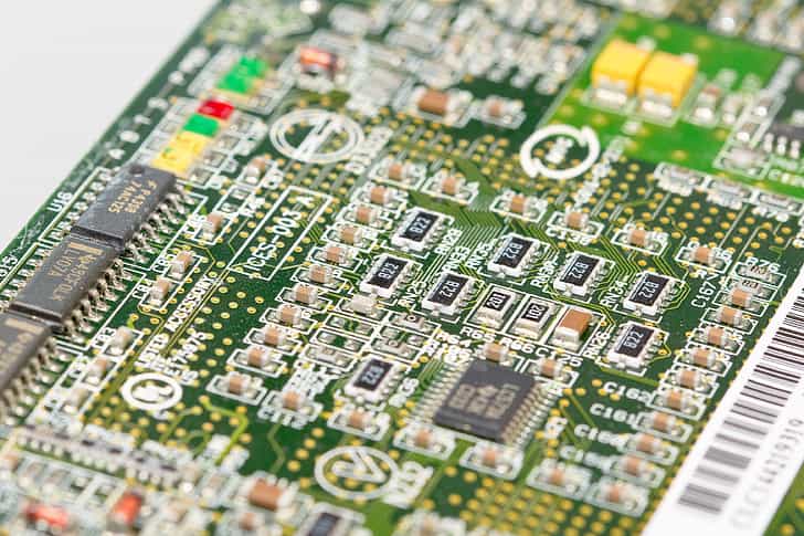
The ITU or International Telecommunications Union considers the high frequency range of electromagnetic waves to extend from 3 MHz to 30 MHz, beyond which, the range extends to VHF or Very High Frequency, UHF or Ultra High Frequency, and more. The electronics industry considers high frequency radio waves as extending from 100 MHz onwards. Rush PCB manufactures RF and high-frequency PCBs for microwaves, mobile phones, and advanced communications equipment working at these frequencies.
High-frequency PCBs differ from regular PCBs mainly in the laminate materials they use, with the materials of the former showing very specific characteristics. Compared to the regular FR-4 material, high-frequency boards use more advanced composites with very specific requisites for dielectric constant, loss tangent, and coefficient of thermal expansion.
Manufacturing high frequency PCBs also requires special skills that a regular manufacturer using standard PCB technology, may not be able to handle. Not only do high frequency boards require a special technique for their design, manufacturers must also fabricate them using special laminates, with attention to specific material options, DFM checks, and high-quality controls that ensure the product performs throughout its life cycle.
Several manufacturers make laminates suitable for high frequencies. Some famous names are Taconic, Polyclad, Isola, Hitachi, Asaki, Metclad, and Rogers. However, different applications have varying demands and budgets, and designers must confer with their contract manufacturers for using the most suitable material that suits both their application and budget.
High-Frequency PCB Features
The simplest way of understanding high-frequency PCBs is by getting to know its features, such as:
- Little or no delay in high-frequency signal transmission—the dielectric constant (Dk) figure must be small and stable—a lower value for Dk ensures more efficient transmission of high frequencies.
- Little or no attenuation of high-frequency signal transmission—the dissipation factor (Df) figure must be small—a lower value for Df ensures low loss and clearer signal transmission.
- No damage due to temperature fluctuations—the coefficient of thermal expansion (CTE) of the substrate material must be very close to that of the copper foil on the board—both should contract and expand equally to avoid separation and prevent electrical discontinuity.
- No damage due to high temperatures—the glass transition temperature (Tg) must be high—to prevent distortion during high temperatures existing in reflow ovens, especially when undergoing lead-free soldering during assembly.
- Appropriate peel off resistance, chemical resistance, water absorption rate, impact endurance, and heat resisting property for the application.
Selecting High-Frequency PCB Material
It is possible to categorize available commercial high-frequency PCB material into seven generic material types. Designers can select the material for their application based on the electrical performance or on the ease of circuit fabrication:
| Material Type | Electrical Performance | Ease of Fabrication |
| High-Performance FR-4 | Poor | Simple |
| Ceramic-Filled Hydrocarbon with Woven Glass | Good | Simple |
| Ceramic-Filled Hydrocarbon | Good | Difficult |
| Ceramic-Filled PTFE with Woven Glass | Good | Moderate |
| Ceramic-Filled PTFE | Excellent | Moderate |
| PTFE with Woven Glass | Good | Difficult |
| PTFE with Micro-Glass Fiber | Excellent | Difficult |
Different manufacturers offer a wide selection of materials for high frequency applications.
- UL Certification, flammability V-0, in accordance with IPC-TM-650
- Low loss factor, Df = 0.0018 at 1.9 GHz
- Excellent peel strength of greater than 10 lbs/in
- Low dielectric constant Dk = 3.5 at 1.9 GHz
- Low moisture absorption factor of less than 0.02%
- Low CTE of 64 ppm/°C in the Z-axis
According to Taconic, RF-35 is an organic-ceramic laminate material. The reinforced microwave material has a base of woven glass cloth and is a combination of glass fiber coated PTFE and ceramic filling technology. The manufacturing technique gives RF-35 an excellent glass transition temperature Tg of 315 °C. The presence of woven glass cloth gives RF-35 unmatched dimensional stability.
The above characteristics of RF-35 make it suitable for use as a low-cost high-frequency laminate material for commercial microwave and wireless frequency applications.
Manufacturing High-Frequency Boards
According to Rush PCB, all laminates above have individual issues with fabrication. Achieving the desired quality and reliability requires following respective fabrication instructions for each material for handling, storing, surface preparation, inner layer preparation, drilling, bonding, deburring, and plating.
Special processes are necessary when fabricating PCBs with HF materials. For instance, preparing for plated-through holes is a critical process, especially for PTFE substrates. PTFE requires a special etch-back process with Plasma etching setup for preparing the hole surface, making it capable of accepting electro-less copper plating. Hence, along with the correct selection of materials, following suitable fabrication methods is equally essential for achieving a board of good quality and working at high frequencies.
Read About: MANUFACTURING PCBS FOR INDUSTRIAL BUSINESSES
Issues with Manufacturing HF Boards
Weak Binding Force: with dense placement of resin-plugged buried vias in the PCB, the binding force between resin and prepreg sheet is low, and may cause de-lamination in these areas after high temperature soldering, reducing high frequency performance. The manufacturer must use plugging resin compatible with the substrate material with comparable CTE and Tg. This allows the two materials to expand and contract in equal measures, reducing the likelihood of de-lamination with temperature fluctuations.
Drilling: A high density of heat dissipating holes in a high-frequency and high-speed multi-layered PCB can be difficult for the fabricator to drill, as regular methods fail to remove the heat generated by the drilling process. This results in melted drilling debris remaining attached to the hole walls, greatly compromising the quality of the hole walls. Drilling high-frequency and high-speed PCB material requires replacing the regular aluminum cover with a resin cover, as it better absorbs heat generated by the drilling process, and increasing the vacuuming and suction pressure. This reduces the drill temperature, keeps the drill lubricated longer, shrinks drilling contaminants, while improving drilling quality.
Back-Drilling: Through holes in a high-frequency board can cause signal integrity problems, as the extra stub of the through hole often acts as a reflecting path, increasing the insertion loss and compromising signal transmission. To solve this problem, the manufacturer must drill a hole larger than the through hole on the reverse side to eliminate the extra stub. However, burrs from the back-drilling process may cause problems. Rush PCB avoids the presence of burrs by drilling prior to etching.
Copper Foil Finish for High Frequencies
High frequency signals never utilize the entire cross-section of the copper track they pass through. As the frequency increases, the flow of signal through the track produces local eddy currents that push the actual current density more towards the outer surface of the track rather than at its center. This makes conductor losses more significant than dielectric losses.
As the current density is higher at the surface, conductor losses increase with an increase in the roughness of the copper surface, when compared with material that has smoother copper conductor surface.
Rush PCB uses smooth conductor layers such as rolled annealed copper that has surface roughness of around 0.3 microns to achieve much better high-frequency performance. High-frequency performance of the PCB degrades with the use of low-profile ED or electro-deposited copper conductor layer with a surface roughness of 0.8 microns, worsening with standard ED copper with surface roughness of 1.8 microns, and high-profile copper with surface roughness of 3 microns.
Therefore, increasing the copper surface roughness while manufacturing can result in increased losses at high frequencies. For instance, a common ceramic-filled hydrocarbon woven glass material, type RO4350BTM laminate from Rogers Corp, shows higher losses when used with a standard high-profile ED copper, while the same material will show much lower losses when it has a low-profile copper layer with a much smoother surface.
Soldermask at High Frequencies
Soldermask when applied on traces carrying high frequencies can increase the dielectric loss of the circuit, as soldermask typically has a higher Df. The loss increases with frequency
Read About: BEST PRACTICES FOR SOLDER RESIST ON PCBS
Thermal Conductivity at High Frequencies
For high-frequency circuits also operating at high power, such as in radio transmitters, an important and necessary characteristic of the PCB material is high thermal conductivity. Micro-fiber PTFE materials naturally have high thermal conductivity, but for others, manufacturers must add a ceramic filler to improve their conductivity.
Conclusion
Rush PCB must consider several issues when selecting material for RF and high-frequency PCBs. While some are fabrication related for achieving the most robust PCB possible, others are meant to achieve the best electrical performance for a given application. As there are various trade-offs, the material for the highest electrical performance for a high-frequency application may not be the same one for fabricating the most robust PCB.


