

Early radio receivers built using valves had a metal chassis for mounting the valves, dials and switches. Engineers placed all other electronic components under the chassis. Since the total number of components were very few, and all were with leads, it was easy to solder them while they hung from terminal boards and interconnect them with wires. However, this procedure became a nightmare when circuit complexity grew and the number of components increased. Using Printed Circuit Boards (PCBs) is a solution to this problem.
Importance of PCBs
Eminent PCB manufacturers such as Rush PCB make PCBs from thin insulating boards with a coating of metal on one or both sides. PCBs hold almost all the electronic components necessary for a device to function. Fabricators etch the metal with acid to create electrical pathways among various components that assemblers mount on the board. Using a PCB brings many advantages to the electronic industry:
- Compact Design
- Ease of Testing and Repair
- Lower Assembly Errors
- Avoiding Short Circuits
- Low Noise and Interference
- Improved Repeatability and Reliability
Compact Design; The ability to mount all components neatly on a PCB leads to a compact design. The PCB designer can experiment with the placement of components on the PCB and their interconnections until they reach an optimum layout that offers the minimum possible size.
Ease of testing and repair: As all the components are on the same plane, applying testing probes for diagnostics is much easier. Locating a faulty component and replacing it is also much simpler, and it is possible to do this without disturbing other components.
Lower assembly errors: Operators made many mistakes when wiring up a complex circuit with components hanging from terminal boards. However, with the introduction of PCBs, it was easy to provide the assembler with a pictorial view of the placement of each component, resulting in a drastic reduction of assembly errors. The cost of assembly also reduced considerably.
Avoiding short circuits: As all electrical connection paths are predefined on a PCB, the chances of short circuits are drastically lower than with manual wiring.
Low noise and interference: The PCB designer can organize the component layout to reduce the electrical noise the circuit generates while operating. They can reduce the path lengths between sensitive components to minimize the pickup of electromagnetic radiation arriving from outside the board.
Improved repeatability and reliability: Manufacturers must follow a specific design to make PCBs, which means PCBs in a production lot are identical. After assembly, each PCB has all the components locked in place and unable to move. This implies repeatability, since each PCB will function almost identically. This is very helpful when producing PCBs in large quantities.
Compared to a manually wired assembly, where it is almost impossible to predict which component is more likely to detach itself, a PCB is far more reliable as it holds all components more securely.
Use the Turnkey PCB services of Rush PCB for all types of PCB design, assembly, and testing for any PCB you require. Call Rush PCB today, or visit our website.
Designing a PCB
Since a PCB holds all the components of a circuit, its design depends on the complexity of the circuit. If the circuit is simple, a single layer board may be enough. As the circuit complexity increases, Rush PCB recommends going for a double-layer board, or using more than two layers, as in a multi-layered board. With a multi-layered board, the designer can keep the total PCB area small. Fig. 1 represents the process flow for designing a PCB.

The process flow shows four major steps in designing a PCB:
- Requirements Gathering
- Schematic Design
- Component Placement
- Routing and Output Generation
Requirements Gathering: this is the input stage and the designer collects information about the intended functioning of the circuit. For instance, the circuit may involve a timer, and the designer must know the minimum and maximum periods the timer will generate, whether the transition from the minimum to the maximum period will be smooth or in discrete steps, and the impedance of the timer’s output. The design requirements may have several constraints that the designer must consider. The designer will choose the necessary components for the circuit based on the above inputs to realize the functionality and address the constraints.
Read About: HDI LAYER STACKUP DESIGN FOR LARGE DENSE PCBS
Schematic Design: in the next stage, the designer draws the circuit and creates an orderly schematic that represents the logical functioning of the circuit. Rush PCB recommends designing the schematic using a PCB CAD (Computer Aided Design) software package. Several such CAD packages are available on the market, starting from free-to-use, to expensive ones.
PCB CAD software packages are usually modular, with different modules capable of handling various stages of PCB design. One such module handles the schematic design, while another handles component layout, and a third module handles trace routing. There may be other modules related to design rule checking. All the modules link to a central library of components that has details of the symbol, the footprint, and many other aspects related to each component. It is important to note that manufacturers often offer the same component in different forms, and the component library of the PCB CAD software package should reflect this variety. However, it is possible to add details of a new component to the library, if it is not present.
Read About: GUIDELINES & BEST PRACTICES IN FLEXIBLE PRINTED CIRCUIT BOARD DESIGN
While drawing a schematic, the designer calls various symbols from the library and places them within the drawing area. They use lines to interconnect the components according to the functionality of the circuit. Fig. 2 represents a typical schematic.
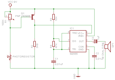
Ref: https://makerobot.files.wordpress.com/2013/01/sss3.png?w=584
.COM
The software module handling the schematic drawing assigns individual part numbers to each component and interprets the interconnections to and from their pins as part of a net. The designer must assign a valid footprint to each part in the schematic.
After completion of the schematic design, the software module offers two outputs—a Bill of Materials (BOM), and a Net List. The BOM is a complete list of all the components the designer has used to build the schematic. The organization uses this BOM to source the components.
The net list is an important document that the designer uses to layout the components for routing. The net list ensures that the designer faithfully transfers all interconnections in the schematic to the layout before starting on the routing.
Component Placement: in this step, the designer uses the net list to download the relevant footprints of each component from the library. For this, they use the component placement module of the PCB CAD software. The designer must carefully select the correct footprint, as a component may be available in several forms such as through-hole and surface mount types.
The designer must place each component such that it can function properly either within the specified boundary of the PCB or within a minimum area. At this stage, the interconnections appear like a maze of lines, as in Fig 3.
Routing and Output Generation: In the final stage, the designer invokes the routing module of the CAD package. This module usually has two parts—the auto-router and the manual router. The auto-router uses algorithms to create traces while routing them through the components. If the designer wants, they can use the manual router to manually create the traces, rather than allowing the computer to create them automatically.
Ref: https://cdn-blog.adafruit.com/uploads/2016/11/F8B5NG4IVA54AHJ.LARGE_.jpg
For a complex design, the designer may have to shuttle between placement and routing until they achieve a satisfactory compromise. On completion, they generate the necessary standard outputs, which they forward for fabricating Primarily, fabricators require Gerber data, drill information, a netlist, and specific fabrication instructions to start manufacturing a board.
Conclusion
The above information is only a brief synopsis on the importance and design of a PCB, as there is much more involved. Rush PCB uses several good practices and design rules to achieve robust and reliable PCBs. They also follow various standards so our PCBs are acceptable across the world.


