

Rush PCB Inc always begin their design of printed circuit boards (PCBs) with appropriate material selection. The goal is always to use the right material for making the PCBs, while meeting the electrical and temperature requirements. With most electronic designs moving towards high-speed, a proper choice of material affects the quality of the signals traversing the board. Therefore, the choice of materials for the board defines the performance and quality of the end product.
The Constituent Materials of a PCB
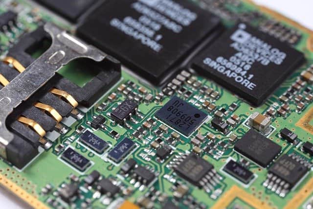
To make a circuit board, manufacturers need the following three items:
Prepreg
This is a reinforcement sheet of woven glass, impregnated with a resin. Typically, this is a B stage material, not fully cured. The tacky material allows bonding of other laminates or foils. Prepreg manufacturers offer them in a variety of epoxy combinations and glass weaves.
Copper Foil
Copper foil present on the outermost layers of the PCB forms the conductive medium for electric signals and current to flow between components. Fabricators make copper traces on a PCB by etching the copper foil, thereby creating electrical connections on the board.
Copper Clad Laminates
Board manufacturers make cores that constitute prepreg laminated and cured with copper foils on both sides. Manufacturers offer a large variety of cores with different thicknesses, types of glass weaves, and epoxy properties. PCB designers define their requirement of combinations best suited for their application.
For making a copper clad laminate, manufacturers use suitable glass cloth of interwoven glass fiber and impregnate this in epoxy resin. They semi-cure this impregnated cloth and bond multiple layers to make up the desired thickness, adding copper foil on the outsides. This forms the copper clad laminate.
Important Properties of PCB Materials
While choosing material for board construction, designers must consider four basic properties of PCB materials.
Chemical Properties
Chemical properties of the PCB material are important as they decide the quality and reliability of the product. Two of the most important chemical properties are:
Moisture Absorption — This is the ability of the material to resist water absorption from the surroundings. Absorption of moisture results in the PCB gaining weight and losing some electrical properties.
Conductive Anodic Filament Resistance — This is the ability of the PCB material to resist forming metallic filaments from electromechanical migrations. These filaments are conductive and may cause electrical shorts on the PCB. Designers must use CAF resistant materials.
Mechanical Properties
Mechanical properties of PCB material determine its ability to withstand external loads and stresses while retaining its characteristics. Three important mechanical properties are:
Elastic Modulus — A measure of the stiffness of the material, defining the amount of force necessary to deform the material.
Bend Strength — A measure of the ability of the material to withstand mechanical stress without fracturing.
Tensile Strength — A measure of the maximum stress the material can withstand without breaking when pulled apart from two sides.
Thermal Properties
Thermal properties of a PCB material determine its ability to withstand extreme temperatures while retaining its characteristics. Four important thermal properties are:
Thermal Conductivity — A measure of the ability of a material to conduct heat. Compared to thermal conductivity of the copper foil, that of the dielectric material is quite low. Therefore, the copper foil removes more heat than the dielectric material of the PCB can.
Coefficient of Thermal Expansion — Rate of expansion or contraction of a PCB material as it heats up or cools down. The PCB material can expand or contract in three dimensions. Typically, the ability of the material to expand or contract along the X and Y directions are quite low. This is because the woven glass constrains the expansion in the X and Y directions. However, the ability of the material to expand or contract in the Z direction is an important parameter.
The CTE of the substrate in the Z direction is generally higher than that of copper, and this can result in interconnection issues as the material heats up or cools down. Therefore, a low CTE along the Z direction is a desirable characteristic of the PCB material.
Decomposition Temperature — This is the temperature at which the PCB material starts losing its mass or it starts chemically decomposing irreversibly. As most PCB materials undergo assembly at temperatures between 200 and 260 °C, where solder melts, the decomposition temperature of the PCB material must be higher than this range.
Glass Transition Temperature — This is the temperature range in which the PCB substrate starts to transition from the rigid, glassy state to a rubbery, deformable, softer state. The change is reversible as the board material cools down.
Electrical Properties
The electrical properties of a PCB material determine its ability to maintain signal integrity around the frequency of operation. Two parameters are of importance here:
Dielectric Constant — The relative permittivity of the material. For most materials, the dielectric constant varies with frequency, decreasing with the increase in frequency. For proper signal integrity at high frequency operation, suitable materials must have a low dielectric constant that does not vary with change in frequency over a wide range.
Dissipation Factor — With increasing frequency, power is lost in a dielectric material. This leads to signal attenuation. PCB materials suitable for high frequency operation must have a low and flat dissipation factor with frequency.
Mechanism of Signal Loss in PCB Materials
At high frequencies of operation, PCB material characteristics can affect the signal integrity. Engineers overcome this by selecting the right type of substrates and copper foil. Signal loss in PCBs is mostly due to losses in the dielectric and in the copper foil. Therefore, these two materials play a major role in causing signal loss in PCBs.
Dielectric Loss
Dielectric materials constitute polarized molecules. Time varying signals passing through the copper traces generate electric fields that cause the molecules to vibrate. The dielectric heats up due to these vibrations, resulting in the dielectric loss part of the signal losses. As molecular vibrations increase with increase in frequency, they cause higher losses in the dielectric. Materials that have a low dissipation factor exhibit lower levels of losses with increase in frequency.
Copper Loss
Eddy currents forming within the copper traces carrying time varying signals, cause skin effect, forcing most of the current flow to the outer surface of the trace. This effectively reduces the area through which the current flows, resulting in the signals facing higher resistance. Skin effect increases with higher frequencies. If the copper trace has a surface finish of nickel, most of the signals might flow through the nickel layer, increasing the signal loss.
Designers can reduce the skin effect by using wider traces, as this increases the cross-sectional area of the trace. But increasing the width of traces may not always be possible.
As most of the outer surface of the traces carry the signals, the roughness of the surfaces also affects the resistance and hence their losses. A smooth copper surface, therefore, reduces signal loss.
Designers must select the copper foil based on the following properties:
Thickness — Typically, the copper thickness varies from 0.3 mils (0.25 oz) to 7 mils (5 oz).
Purity — Electronic grade copper is around 99.7% pure.
Copper-dielectric Interface Profile — A low profile offers lower copper losses for signals at high frequencies.
Basic PCB Material Types
Depending on the loss factor and the speed of operation, there are four basic PCB material types:
Normal Loss and Normal Speed
These are the most common type of PCB materials available. Isola FR370HR and the FR-4 family of materials fall in this category. With higher dielectric losses, these materials also do not show a flat dielectric constant versus frequency. Therefore, these materials are good only up to a few gigahertz of digital or analog applications.
Medium Loss and Medium Speed
Exhibiting a somewhat improved flat dielectric constant with frequency and half the dielectric loss of normal speed materials, medium speed materials are suitable for applications nearing 10 GHz. A good example of this type of material is the Nelco N700-2 HT.
Low Loss and High Speed
With significantly low dielectric loss and flatter dielectric constant with frequency, these materials are suitable for applications operating between 10 – 30 GHz. Low loss and high speed materials also generate lower levels of unwanted electrical noise in comparison to other materials. An example of such a material is the Isola I-Speed.
Very Low Losses and Very High Speeds
These materials are suitable for applications in the RF/Microwave frequencies. They exhibit the least dielectric loss and the flattest dielectric constant with frequency. They are suitable for frequencies of operation from 20 GHz and above. A suitable example of this type of material is the Isola Tachyon 100G.
| Application Area | Material | Performance |
| Normal Loss, Normal Speed | Isola — FR370HR | 0 – 10 GHz |
| Medium Loss, Medium Speed | Nelco — N7000-2 HT | 0 – 10 GHz |
| Low Loss, High Speed | Isola — FR408HR | 10 – 30 GHz |
| Isola — I-Speed | ||
| Panasonic — Megtron6 R-5775 | ||
| Isola — FR408HR | ||
| Very Low Loss, Very High Speed | Isola — I-Tera MT40 | 20 – 60 GHz |
| Rogers — RO3003 | ||
| Rogers — RO4350 B | ||
| Isola — Tachyon-100G | ||
| Isola — Astra MT77 |
Types of Copper Foil
Rolled Copper Foil
Mostly used by fabricators for making flexible PCBs, this type of copper foil is very thin as they are processed by rolling them between heavy rollers. The smooth surface and the horizontal grain structure resulting from the rolling makes rolled copper very suitable for low loss and high speed PCBs.
Electro-Deposited Copper Foil
With a rough surface and vertical grain structure, this type of electro-deposited copper foil is useful for rigid PCBs operating with normal loss, normal speed applications.
Low-Profile Copper Foil
Organic additives or levelers added to the plating bath of electro-deposited copper foils help in reducing the roughness.
Best Practices in PCB Material Selection
- Select low moisture absorption materials
- Select CAF resistant materials
- Select substrates with a tight weave
- Always match the CTE
- Do not use FR4 for high frequency and high speed designs
- Follow IPC standards:
- IPC-4101C — IPC standard specifications for PCB base materials for rigid, multi-layered boards.
- IPC-4103 — IPC standard specifications for PCB base materials for high-frequency/high-speed applications.
- IPC/JPCA-4104 — IPC standard specifications for PCB base materials for HDI and Microvia boards.
- IPC-4204 — IPC standard specifications for flexible and metal-clad substrates.
Conclusion
Eminent PCB manufacturers like Rush PCB Inc have been using specialty high-frequency/high-speed circuit materials for decades and for different reasons. These materials have several unique attributes as compared to that of the more traditional PCB materials. By understanding these attributes, OEMs and PCB fabricators can not only improve circuit performance, but also benefit greatly from them.


