

Printed Circuit Board (PCB) manufacturers typically follow three types of stackups for boards they will assemble with high-density packages:
- Standard Lamination with Vias or Plated Through Holes
- Sequential Lamination with Plated through, Blind, and Buried Vias
- Lamination Buildup with microvias
Among the three above, the last is especially suitable for High Density Interconnect PCB (HDI PCB). Rush PCB Inc., eminent HDI PCB manufacturer,recommends using lamination buildup with microvias for HDI printed circuit boards that have high pin-count Ball Grid Arrays (BGA) and other fine-pitch packages, as each type has its own advantages and disadvantages.
For instance, standard lamination with through vias may be low cost for 28 layers and below, but is very difficult to route when multiple BGAs with over 1500 pins and less than 0.8 mm pitch are involved. Likewise, sequential lamination with blind and buried vias have potentially shorter via stubs and fairly simple via models, with smaller via diameters than those required for through hole vias. Costing more than the standard lamination with through vias, sequentially laminated boards maintain the same minimum trace widths and their practical reliability limits their number of layers to a maximum of two or three.
Above limitations and more are leading to a larger number of HDI PCB manufacturers moving towards building up laminations with microvias and other advanced features for HDI PCBs. Advantages of the microvia HDI PCB design include achieving very high route density with fewer layers, as the traces and vias have much smaller dimensions comparatively. In microvia HDI PCBs, the potential for a lower number of layers comes from the effective use of patterns with microvias, as this opens up more space for routing, providing the only applicable way of designing with several large, fine-pitch BGAs with pitch measuring 0.8 mm or lower.
Offering the lowest cost for high frequency, high-density boards, HDI technology, with suitable stackup definition, also improves power and signal integrity in high frequency PCBs. Although typical materials fabricators use for HDI PCBs do well in processes requiring RoHS, use of newer materials has the potential of higher performance with the lowest costs. Notably, these newer materials are not suitable for fabrication of boards using standard or sequential lamination.
HDI PCB Stackups
Based on the IPC-2315 standard from the Institute of Printed Circuits (IPC), fabricators may use HDI PCB stackup of types I, II, III, IV, V, or Vi. Of the above, types IV, V, and VI are more expensive to fabricate and usually not suitable for high density PCBs with challenges of routing and BGA breakout.
The standard differentiates HDI stackups with the use of via types—micro, blind, and buried, along with plated through vias, although use of the latter is not strictly necessary for flex PCBs.
HDI Type I
HDI PCBs of Type I stackup have a structure of a laminated core with at least a single layer of microvias on one or both of its sides. Type I HDI may use PTH vias and blind vias, but no buried vias.
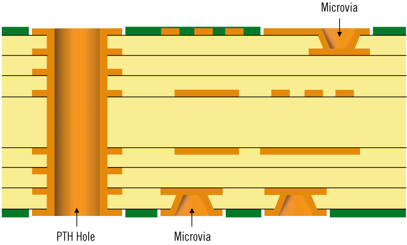
Two factors limit the number of layers in the laminated core of Type I HDI PCBs:
- The aspect ratio or total length to hole diameter for the plated through hole (PTH) via must be less than 10 to maintain reasonable reliability.
- Very thin FR-4 dielectrics can delaminate under high temperatures required for lead-free soldering.
Therefore, Type I HDI stackup will not be significantly better than the laminate for large dense boards with multiple pin-count BGAs, as the PTH via pads will need to grow larger for higher layer counts. Moreover, the use of a single microvia layer does not offer appreciable benefits with the introduction of special features such as smaller diameter vias and thinner traces.
HDI Type II
HDI Type II structure construction uses microvias, blind and buried vias on a laminated core, with at least a single layer of microvias on one or both sides. Fabricators may stagger microvias from other microvias, and stack them or stagger them relative to buried vias.
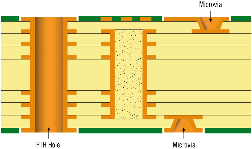
Although the HDI PCB Type II stackup is significantly better than Type I for large dense boards using multiple fine pitch components, it has the same limitations as that of the Type I in context of the limitations on the number of laminated core layers.
As Type II HDI PCBs can have microvias only on their outermost layers, it places restrictions on using the outermost layers for a ground or power plane. Additionally, it is not very effective when there is only a single buildup layer for trace routing.
HDI Type III
HDI Type III structure construction also uses microvias, blind and buried vias on a laminated core, with at least two layers of microvias on one or both sides. Fabricators may stagger microvias from other microvias, and stack them or stagger them relative to buried vias.
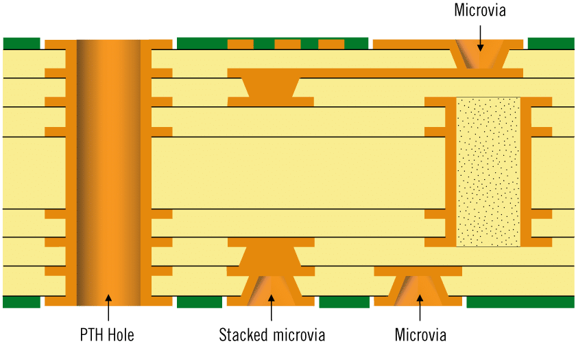
Type III HDI PCBs offer the best stackup configuration for large dense multilayer PCBs using multiple large fine pitch BGAs, although they have the same limitations on the number of layers as faced by Type I and II when they use PTH holes and thin FR-4 dielectrics.
Using microvias in the inner layers of Type III HDI PCBs allows the outer layers to be used for ground and/or power planes, leaving adequate number of layers for signal routing. Additionally, designers can attain greater routing density with stacked vias, but at higher cost.
Summary
Depending on the application and available budget, designers may use any one of the three types of High Density Interconnect PCB stackup. Type III microvia HDI PCBs offer the widest type of via models and spans. Fabrication cost will depend on the best via models that accommodate the highest route density and signal integrity.


