

For increasing their market share, OEMs are resorting to bringing out new products and reducing their time-to-market. However, with component packages getting smaller, assembly designs getting denser, and assembly process margins getting tighter, Printed Circuit Board (PCB) designers are facing increasingly tougher challenges. Designers need to resort to specific checks at each step of the design to ensure the final product will function as intended.
The designer is not the only person involved in the PCB industry. Fabricators and assemblers also play their individual crucial roles. Fabricators manufacture the bare boards, while assemblers mount components on them. If everything goes well, the board starts functioning. However, depending on chance is a risky and expensive way for OEMs to make products that depend on PCBs to function properly. To mitigate the risk and reduce the expenses, Rush PCB recommends designers, fabricators, and assemblers to resort to Design for Assembly or DFA and Design for Manufacturing or DFM analysis before start of production.
Read About: IMPORTANCE OF DFMA PROCEDURES FOR PCBS
By following DFA and DFM techniques, designers can arrange the topology of a PCB they are designing to mitigate problems that the fabricator and the assembler may encounter during the fabrication and assembly processes. While DFM addresses problems that fabricators may face when fabricating the PCB, DFA addresses problems that assemblers may face when assembling components on the PCB. Together the two mostly make up the DFMA analysis.
DFM Analysis
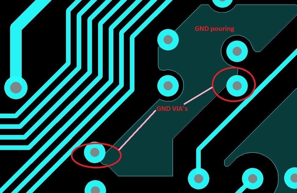
Several factors are important to the fabricator in charge of building up a PCB. The designer mainly conveys the information in the form of electronic documentation as Gerber files. The information provides details on the board materials and properties, the stackup, copper information of each layer, drill details, aperture details, net list, surface finish, plating finish, soldermask and silkscreen information, assembly information, test point details, and details on the panel design.
The designer generates the above information to ensure that the board is manufacturable. The manufacturer runs a DFM analysis on the information available to ensure that with their existing capabilities they can manufacture the board.
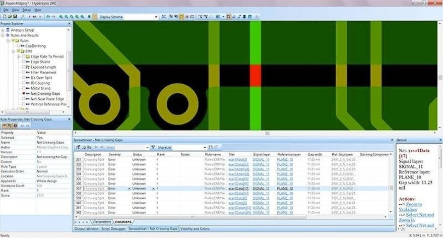
During the DFM analysis, the manufacturer may discover a potential problem that could seriously hamper the production process. The PCB manufacturer may discuss the issue with the designer and offer a solution.
For instance, through DFM analysis the manufacturer may discover sharp bends in traces on a layer that can possibly trap acids during the board etching process. The trapped acid can over-etch a connection, resulting in a defective circuit. The solution is to replace all sharp bends with shallow ones.
Manufacturers using automated machines to fabricate PCBs require an extra area on either side of the board for handling. If the design information provided does not contain this extra handling area, DFM analysis will flag this as a potential problem.
DFA Analysis
The scope of DFA analysis differs from that of DFM, although many of the strategies are interchangeably applicable in a general sense to all areas of PCB design. Related to the components that will go on to the PCB for mounting, DFA analysis mainly considers reduction and combination of components, their standardization, minimization of risk, simplification, clarity, and an understanding of the capabilities of the assembler.
Although each of the above points are very important for assembly, the final strategy is the most explicit, as it decides the ability of the designer to achieve the remaining. For instance, if the designer has specified the use of 0201 SMD packages, the assembler must have pick-n-place machinery capable of handling such small packages.
DFA analysis can help in improving the reliability of the PCB assembly. The analyst checks the source of the components that should have come from reliable manufacturers with assurances of accuracy, stability, and reliable delivery. For instance, if a manufacturer has marked the status of a component as obsolete or end-of-life, the designer should rather use a suitable replacement instead.
DFMA Analysis
Until recently, OEMs left both DFM and DFA analysis to the PCB fabricator and assembly engineer to manage. PCB designers would be content to run a Design Rule Check or DRC before submitting their design for manufacturing.
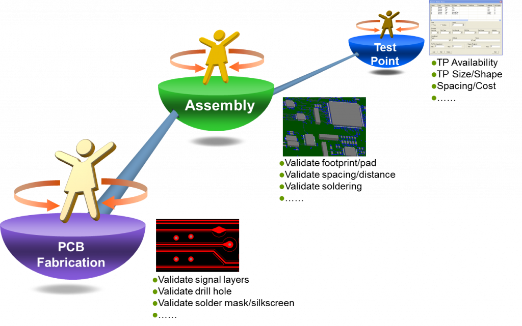
Eminent manufacturers such as Rush PCB, aware that issues such as slivers, acid traps, starved thermal pad connections, via in pads, and more can reduce manufacturing yields and increase costs, took upon themselves to use DFMA techniques to analyze the design. Although this ensured they built the design with the lowest cost and maximum yields, there were several reasons for moving the DFMA analysis into the PCB design flow.
Conclusion
Rush PCB recommends moving DFMA analysis to the start of the PCB design, together with a close consultation with the PCB manufacturer. This ensures weeding out potential pitfalls before they can grow to unmanageable sizes. The advantages to the OEMs is significant. It leads to a drastic reduction in the cost of finished PCBs, the potential for failure in future designs, and an ability to maintain the design intent.


