

Identifying both hot and cold spots on the PCBA are very important to set up right reflow profile as the Conveyor speed in the oven should allow both the hot and the cold spots to reach equilibrium by the time the PCBA assembly reaches the end of the preheat phase. In the reflow phase, the solder melts to form reliable soldered joints:
Here are the few step to identify the Hottest and coldest spot on the PCBA
- The temperature solder joints reach, and the time above melting point of the solder, are a combination of three factors:
- Thermal mass of component.
(Larger thermal mass = lower maximum temp. = less time above melting point)
- Proximity of component to components of high thermal mass
(Nearer to high thermal mass component = lower maximum temp. = less time above melting point)
- Proximity to edge of assembly.

Nearer to edge = higher maximum temp. = more time above melting point
- Therefore the coolest solder joints will usually be on large components, close to other large components towards the centre of the assembly. Hottest solder joints will usually be smaller components, in less densely populated regions of the assembly, closer to the edges of the assembly.
- Thermocouples should be attached to solder joints that will show both the hottest and coldest parts of the assembly, to ensure that all joints reach a temperature in excess of the melting point of the chosen solder and that no part of the assembly is getting so hot that irreparable damage can occur. If the hottest and coldest parts of the assembly have not previously been identified, it is recommended that measurements should be taken from at least six positions on the test assembly.

Why hot spot and cold spot???
| Component | Volume mm3 | Area mm2 | Volume/Area mm |
| CO603 | 1.02 | 40 | 0.026 |
| Board 141*208*1.6 | 46925 | 58656 | 0.8 |
| PLCC68 | 11250 | 5550 | 2.03 |
>> Huge difference in thermal mass in the BOM
While maintaining a 235°C minimum solder joint temperature (= coldest spot), hottest spot might be well reaching the critical (potential) thermal damage limit.
Determination of hottest spot and coldest spot for top side
1. Apply solder paste on top side of printed board
2. Mount all components on top side of the board
3. Adjust oven to (*):
4. Pre-heat zones: as normal settings (+/- 160°C) Reflow peak zones: as normal setting (+/- 280°C) Conveyor speed “full speed.
5. Allow oven temperature to stabilize
6. Pass board through oven
7. Check: any paste dots molten?
8. If no: decrease transport speed (e.g. with 0,05m/min) if yes, go to step 9
9. Repeat steps 5, 6 and 7.
10.Pass a board max 4 times through an oven, apply some flux with small brush for next pass (next 4 passes max) on.
11. Take a new board with paste and components, when close to the hottest spot
12. If some paste dots are molten: only a few dots (say < 10)
13. These dots are called Hot Spots (HS)
14. If too many dots, go to next step
15. If (too) many dots are molten: take new board with paste and components
16. Increase speed with very small steps (0,01m/min), allow oven to stabilize
17. Repeat steps 5, 6, 7 and 8
18. Now the Hot Spot(s) is/are known
HOT SPOT: how to recognize?
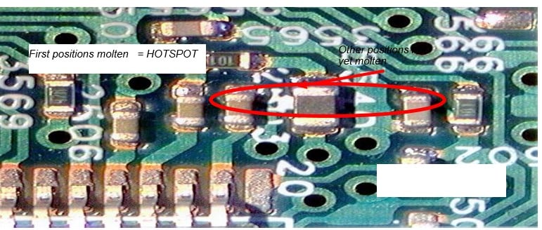
- Decreased speed of transport (with 0,05m/min)
- Pass board through oven
- Are all paste dots molten?
- If no, repeat steps 14, 15 and 16
- If only a few (say < 10) dots are still not molten
- Cold spot (to verify, repeat steps 14, 15 and 16)
- If ALL are molten, go to next step
- If all dots are molten: take new board with paste and components.
- Increase speed with very small steps (0,01m/min).
- Repeat from step 15 onwards.
- Now cold spot known.
Determination of hottest spot and coldest spot for bottom side:
Same procedure as for top side BUT
All components on top side also mounted!
REQUIRED MATERIALS (rule of thumb, but pending):
- Single Sided reflow board: For HS / CS determination on top side 1:to 3 boards
- Double Sided reflow board: For HS / CS determination on top side and
Bottom side:2 to 6 boards (2 for each side)
Determination of hottest spot and coldest spot requires up to 4 hours for one (1) board side!!!
SO: DS reflow board requires up to 8 hours!!!
Such activities should be considered as an investment for later smooth processing/control
Rule of thumb: Follow profile advice of solder paste supplier, but take into
Account also the limitations of your components and PCB!
For High Temperature Organic Solderable Protective (HT-OSP) coatings it is recommended to use a nearly straight ramp profile, to minimize the thermal load on the OSP coating during reflow soldering.


