

Improvements in laminate materials, routing density, and assembly techniques continue to drive the evolution of printed circuit boards or PCBs from eminent PCB suppliers such as Rush PCB. A metallization process is at the core of these PCBs, necessary for making the drilled holes conductive, thereby creating interconnections for achieving the functionality of the finished board.
High volume manufacturing lines in Rush PCB, as in many of the world’s leading PCB industries, use the electroless copper plating technology as an essential process. Achieving interconnect reliability is one of the critical challenges this technology faces. Rush PCB achieves manufacturing control with a superior understanding of material interactions.
Whether the hole drilled in the PCB laminate is made by a laser drill or a mechanical one, to provide conductivity across the dielectric laminate material, the PCB fabricator uses an electroless copper process. The fabricator must ensure the electroless copper process covers the dielectric material while providing reliable inner-layer interconnections. One of the factors adversely affecting interconnect reliability is poor copper adhesion and these causes interconnect defects or ICDs.
Reliability of Interconnections
As overall PCB performance hinges on interconnect reliability, it is imperative to understand the materials and the chemical and mechanical processes necessary to manufacture circuit boards—for ensuring their best possible reliability.
For instance, most board materials in use have coefficients of thermal expansion or CTE higher than copper does. Therefore, exposing the PCB to elevated temperatures during the assembly process makes the dielectric expand more than the copper can, thereby increasing the stresses at the inner-layer interconnections. Consequently, unless there is good adhesion between the inner-layer copper and the copper plating in the through-hole, the two can come apart, leading to ICDs.
ICDs may lead to the failure of a specific circuit or net on the PCB. Typically, such failures are mostly of the open circuit type, but they could also be of the intermittent type, aggravated by high temperatures, leading to reliability issues.
Reliability of interconnections is a significant concern, as the functionality of the PCB may remain good while it is fabricated, and failing during assembly or actual use. This latency of the defects makes ICDs a reliability risk, with the industry treating them as high-priority serious defects.
Detecting ICDs
To detect ICDs, PCB manufacturers typically use quality control checks of coupons from working panels after the plating process, usually after circuit formation. Rush PCB also uses thermal stress testing, typically in the form of solder float testing, to detect ICDs. This consists of multiple solder floats at temperatures of 288°C or higher, depending on the PCB material in use.
After the thermal stress testing, evaluation of microsections by optical microscopes leads to the detection of presence of failures. Rush PCB has developed protocols for both thermal cycling and thermal stress such as with HATS or IST testing. These help to quantify ICD performance based on evaluation using experiments with different materials and process conditions.
Causes of ICDs
Thermal stress can bring out three types of ICDs occurring in multi-layered printed circuit boards, formed due to various causes:
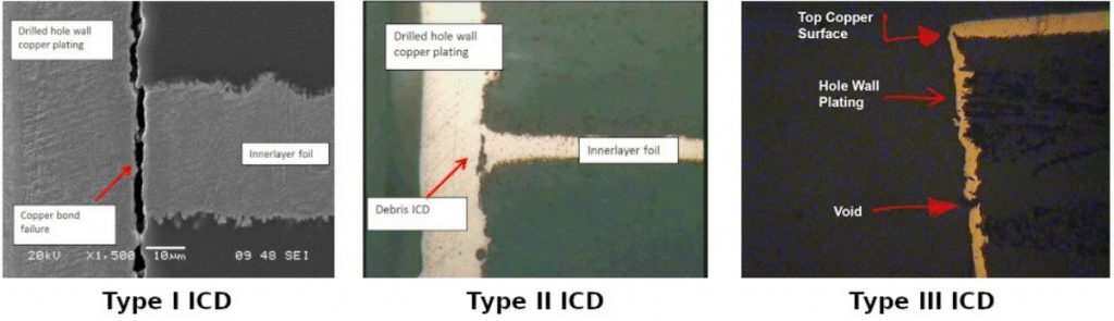
Type I: This type of ICD is the separation present at the interface of electroless copper and inner-layer copper. This is also known as the copper bond type ICD. The primary cause is poor controls within the electroless copper process.
Type II: This type of ICD is the separation present at the interface of electrolytic copper and electroless copper, mainly caused by debris from drilling, residue from post-electroless copper cleaning, contamination from pre-treatment prior to electrolytic plating, or inadequate control over the electrolytic copper processes.
Type III: This type of ICD is the separation present within the electroless copper layer itself. This is mainly caused by poor controls in the electroless copper process.
Debris from drilling or material left behind after the hole-drilling process, drill smears, and particles of glass and inorganic fillers remaining embedded within the interlayer copper surface, unless removed effectively, are a major cause for ICDs.
Formation of vias, both mechanically drilled for through-holes and laser-drilled for micro-vias, generates considerable localized heat along with resin-containing debris appearing as smear on the capture-pad or inner-layer copper surfaces. Unless completely removed before starting the electroless copper process, this smear can eventually form a barrier between the copper surface and the subsequently plated copper, resulting in ICD.
ICDs caused by failure of copper bond occurs when the copper connection breaks physically. Typical reasons for this are high stress generated during assembly or use, or the copper bond being weak, or a combination. Sometimes, this failure mode can be linked to design, as increasing PCB thickness, increasing hole size, and use of wave soldering tend to increase the risk from copper bond ICDs.
Another cause of ICDs is the increasing use of lead-free soldering, where the temperatures are higher than those involved in regular leaded solder usage. This, in conjunction with increased board thickness over the past decade, has led to an increase in the occurrence of ICDs.
Incidentally, ICDs also plague HDI microvias. Although the causes are similar, the processing conditions are different.
Preventing ICDs
Rush PCB removes the smear using either a de-smear wet-chemical process or a plasma etching process. In both cases, we evaluate the effectiveness of the de-smearing process for each type of laminate material we use. For improving the physical and electrical properties of high-speed, high-Tg laminate materials, laminate manufacturers add both organic and inorganic filters. Increase in ICDs of this type is related to the increasing use of inorganic filler types for low Dk/low Df materials, as these materials generate more drilling debris, often more resistant chemically compared to standard FR-4 epoxy materials.
Addition of fillers changes the machinability of the laminates, and this calls for evaluation of drilling and de-smearing processes to maintain their effectiveness. Filler material not effectively removed can remain embedded within the inner layer copper surfaces, and may lead to ICDs. Rush PCB detects the use of fillers by the presence of elements such as calcium, aluminum, and silicon. We also use techniques such as XPS and/or EDS for identifying ICDs of this type by analyzing the elemental composition of the area of defect.
Reliability testing at Rush PCB has established copper bond type or Type I ICDs are a significant reliability issue, showing up as assembly failures and products with weakness and a tendency for field failure. On the other hand, Type II ICDs, while not a significant reliability issue, are an industry specification failure affecting product yield and costs. At Rush PCB, we use a valid coupon structure to run IST testing, and have established this as a valuable testing method for determining risk from ICDs.
While good PCB design along with improved PCB processing methods can prevent ICD Type I and III, proper de-smearing and drilling parameters can help prevent ICD Type II. Some of the newer material with fillers have different machinable properties compared to standard FR-4. Rather than chipping during drilling, they tend to break into small particles that coat the drilled hole walls.
While drilling, drill bit heating tends to increase debris formation and thereby increase the risk of formation of ICD Type II. This requires aggressive de-smearing to remove drilling residues, to be effective in reducing or eliminating ICD Type II.
Preventing Type I and III ICD failures is more complex. During PCB processing, it is necessary to clean the copper surface at inner layers thoroughly for allowing a strong bond formation. Additionally, there must be a good control over the electroless copper deposit to achieve the proper thickness and grain structure, and to acquire the required strength. With extensive testing and experience, Rush PCB has established that a good processing focus accompanied by reliability testing results in a consistently robust product.
Read More: How ESD Affects PCBs?
As noted above, design factors also play a significant role. For instance, hole size and board thickness are two key factors. Their main relation is to the stress levels existing on the interconnects during thermal exposure. One of the major ways Rush PCB has been able to avoid this issue is by eliminating soldered through-hole connectors. For thick boards, Rush PCB prefers to use materials with lower z-axis CTE and high Tg values to effectively reduce the stress.
Conclusion
As demand for PCB performance continues to rise, ICDs remain an issue. Reducing the impact that ICDs have on the performance of the boards is only possible by designers gaining a better understanding of the failures. Rush PCB uses superior PCB processing practices in drilling and de-smearing along with proper electroless copper technology to improve the quality of boards. Rush PCB also implements industry best practices, thereby reducing opportunities for ICDs.


