

Rush PCB Inc. is one of the most advanced PCB manufacturers. We also make fully assembled PCBs. Most people are mystified when confronting a fully assembled PCB. Although it looks more like a board with decorations on it, it is in fact a printed circuit board with several small electronic components mounted on it. Such boards with components mounted on them are known as assembled printed circuit boards and they undergo a special PCB components assembly process to make them functional.
The PCB components assembly process involves several automated and manual steps. Each manufacturer can select to use either the manual step or an automated step depending on the complexity of their floor setup. Assemblers may use various component types for the assembly, such as:
- Through-Hole PCB Components
- Surface Mount PCB Components
- Mixed PCB Components
Each of the above component types has their own assembly processes. Starting from the PCB fabrication and until the final soldering, assemblers must follow these processes to achieve a high-quality PCB assembly.
Through-Hole PCB Components
These are components with long leads and are a generation behind surface mount components. To use these components, the assembler must insert the leads into holes in the board and solder them on the underside. Typically, the PCB components assembly process for boards using only through-hole components mount them only on the top side of the board.
PCB Design
Designing PCBs with only through-hole components requires placing holes for all the leads at distances specified by the component manufacturer. For a single-layer board, these holes are not plated through. Multi-layered boards need plated-through holes for component mounting, and these holes can also act as vias for connecting circuits on the outer layers to those on intermediate layers.
As the board requires drilling of several holes, the area available for routing traces reduces drastically. That means the board must have a larger area for accommodating all the connections, or it must have a higher number of layers in the stackup.
Component Mounting
The fabricator may follow a manual process for component mounting or use automated machinery. In both processes, the component leads need pre-processing before insertion. This requires the leads to be cut and bent to facilitate easy insertion. The automated process may clinch the leads to prevent the component from falling out.
Soldering
The most common process of soldering through hole components is by wave soldering. The soldering machine typically uses a nozzle through which a pump pushes up molten solder. As the PCB components assembly passes over the molten solder wave, it touches the leads and the pads on the underside of the board, soldering them in place.
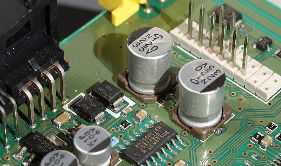
Surface Mount PCB Components
These electronic components have very small, non-protruding leads and do not require holes in the board to mount them. Being very small, it is possible to pack them close together on the PCB for achieving highly dense assemblies. For printed circuit boards using surface mount components only, it is possible to mount them on both sides of the board.
PCB Design
As the designer does not need to reserve space for holes for mounting surface mount components, they can achieve much higher component density. This results in a smaller board, and in case of multi-layered boards, a lesser number of layers in the stackup.
Designers can achieve very high densities by using very small size vias with surface mount components. They can also use tented vias in pads for fine pitch components like BGAs. However, as the size of these components is very small, designers must pay adequate attention to the size and spacing of their pads.
Solder Paste Deposition
Before mounting the components, the assembler must deposit solder paste on the pads. For this, they use a stencil with proper openings. The solder paste deposition may be a manual process or an automated one. A metal squeegee pushes the solder paste across the stencil placed atop a printed circuit board. The solder paste passes through the openings in the stencil and deposits on the pads.
Component Mounting
While it is possible to manually mount large surface mount components, a special pick-and-place automated machine is necessary for mount most of the smaller ones. Manufacturers supply surface mount components in reels, tapes, trays, and tubes. Pick-and-place machines accept such packing and use a suction head to pick the individual component. The machine has a program for mounting each component in its location on the board with solder paste on the pads.
Soldering
As solder paste is already present between the component and the pads, the soldering process only needs to apply adequate amount of heat to melt the solder for anchoring the component in its place. Assemblers use a reflow soldering machine for the purpose.
The reflow soldering machine uses infrared heaters to generate the necessary heat on the boards. As the PCB components assembly passes through the reflow machine, heat melts the solder paste fixing the components to the pads.
Mixed PCB Components
Although manufacturers offer most through-hole components in their surface-mount packages, some applications must use a mix of through-hole and surface mount components for their PCB assembly.
PCB Design
To make the assembly process simpler, designers place surface mount components on the underside of the board. This allows the wave soldering process to solder them along with the through-hole components.
Component Mounting
However, when mounting the surface mount components, the assembler must replace the solder paste deposition process with a glue deposition process. A dispenser places a tiny drop of glue between the pads of the component before the pick-and-place machine mounts the surface mount components. The board must undergo a curing process for the glue to harden and hold the component.
Soldering
The assembler can now turn the board over to insert the through-hole components. The entire assembly then goes through the wave soldering process.
Advantages and Disadvantages
While through-hole components seem simpler for assembly of PCB components, it is a difficult process to control and has several opportunities for failure. The wave soldering process often causes solder shorts when adjacent component leads are close. Moreover, through-hole components do not allow high density assembly that most modern equipment try to achieve.
Surface mount components overcome many of the problems assemblers face with through-hole components. Being significantly smaller, it is possible to pack surface mount components close together, thereby creating very high component density on the printed circuit board. The reflow soldering process allows a much higher level of control, resulting in a significantly higher quality of soldering compared to that from the wave soldering process.
Assemblers prefer avoiding mixed components for PCB assembly because of the complexities in the assembly process, and the shortcomings of the wave soldering process necessary.
Conclusion
According to Rush PCB Inc., PCB components assembly is an important process for producing a successfully working printed circuit board. With numerous component manufacturers offering a huge variety of surface mount components in myriad packages, designers and assemblers can exercise their choice according to their requirement. Soldering is a crucial step in the components assembly process, and it is necessary for the operator to set the oven to the optimum profile for the specific board and components.


