

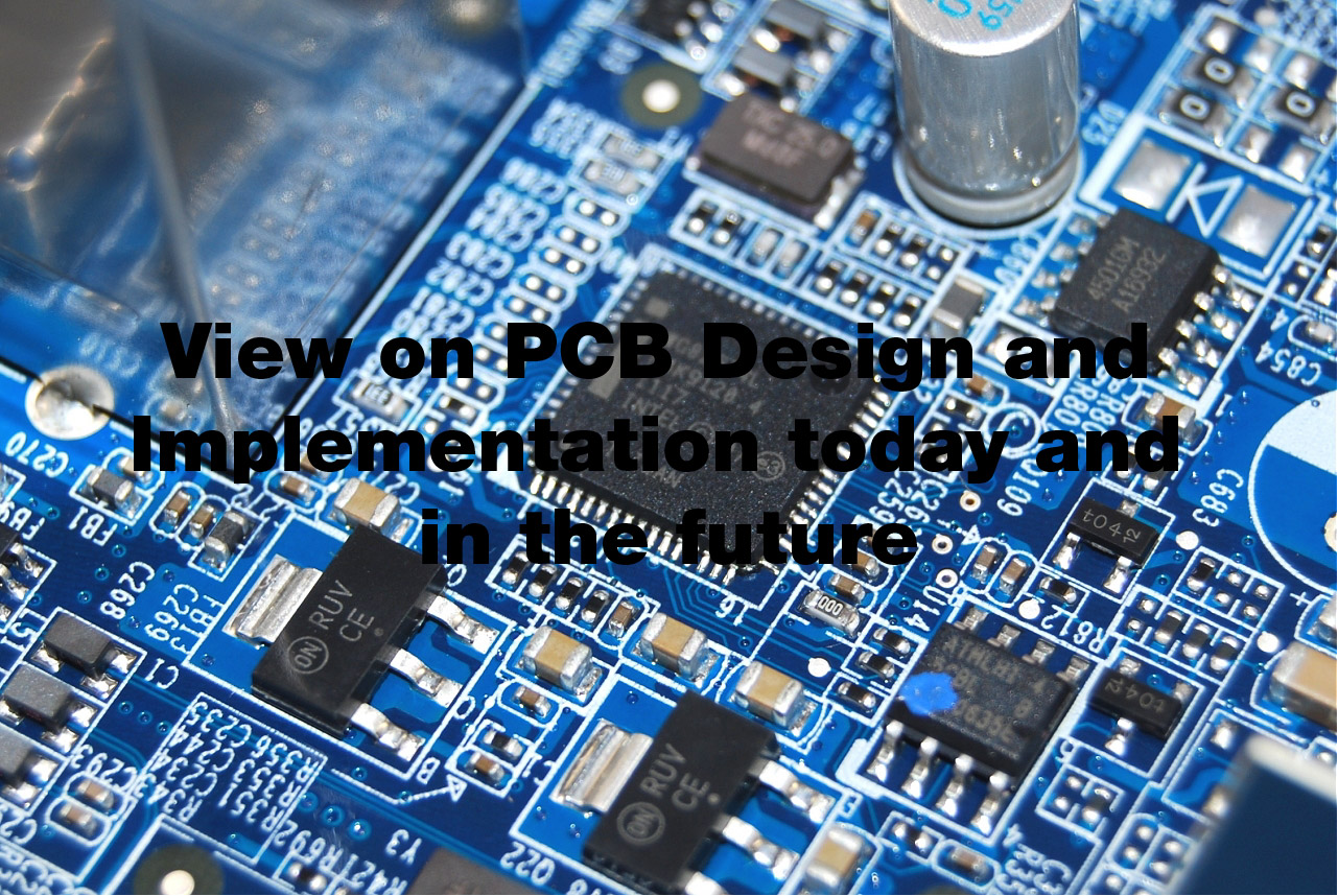
PCBs are the cornerstone of just about all modern electronics, and they evolve along with the rest of the field. So what is the future of the PCB? The first things we’re likely to see is PCBs shrinking to meet the increasingly intense demand for thinner, lighter, and more powerful electronics. But these changes are just the tip of the iceberg. It’s also possible that we’ll see PCBs take a more active role in their devices. Currently they act as relays of a sort. They’re designed to carry electrical current, but what if they could take a more active role? As technology progresses we’re going to start even more seeing integrated logic and other components within PCBs themselves. This isn’t entirely new technology, but as implementation improves we’re going to see it making a huge difference in how devices function. It is vastly more efficient to have components integrated into the PCB because travel time for currents can be reduced, and even more importantly manufacturers will be able to cut down on wasted space within their designs. This technology is also going to allow for leaps in asynchronous processing which will allow for faster transfer speeds. Already we see transfer speeds on the order of several gigabits. We are rapidly approaching the point where PCB optimization is critical to creating good devices.
The Future lies in 3D printing
R&D will be critical but of course even the best technologies can fall by the wayside if they’re not economical enough or easy enough to manufacture. This is where emerging technologies like 3d printing will shine. We’ll see printers printing with conductive materials and manufacturing PCBs far more efficiently than would ever have been possible with more traditional laminated frameworks. 3d printers are now becoming capable of printing copper and other materials, and they can do so onto almost any materials. As a net effect this means that it will become far easier to implement cheap electronics into just about any household object. Printing PCBs with this method could cost as little as $50 for each meter of printed electronics. But although these 3d printed structures are cheap and easy to implement they can lack efficiency. They can be made complex, but for the moment complex 3d printed PCBs are difficult to produce in large volumes.
If you want to see the future of PCBs it is here already with Micro Electronic flex boards with 1 mil lines and spaces
Additionally, PCBs can be flexible, transparent, and durable. There flex and rigid flex PCBs as well three dimensional PCBs. There are also rolled flex boards that can be up to 30 feet long. There are also very sophisticated PCBs. Microvias for example, are used in a number of applications interconnecting the fused layers in PCBs and creating far denser circuits capable of accepting more complex components. This is just another innovation which will allow for smaller and more efficient PCBs. In summary. PCBs will continue get faster, smaller, and more efficient in the short term, but what is in store for us longer term? Here is a safe bet, things will get smaller and more complex. If you want to see what PCBs will look like in the future look at Micro Electronic Circuits such as the ones that go into very advanced hearing aids and in medical electronics such as a diagnostic capsule that you swallow and the boards that go into ultrasound wands. These are tiny flex boards with 1 mil lines and spaces. Now that’s the future.


