

As Rush PCB makes increasingly smaller printed circuit boards or PCBs, we are using fewer through hole components, while using more of surface mount technology or SMT components. Accordingly, we are allocating less of the precious space on the board for relatively large plated through holes. With the increasing use of SMT components, rather than plated through holes, our modern PCBs are using more vias.
Vias are Useful
Vias on a PCB are holes for electrically connecting stacked pads on different circuit layers. A plated hole wall allows electrical signals to travel from one circuit layer to another. Although all vias essentially perform the same function, there are different types depending on their appearance on the PCB surface.
Types of Vias
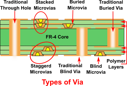
Traditional PCBs use mechanically drilled vias, of which there are three types—through, blind, and buried.
Through Vias: The fabricator drills through the entire stack from the top layer, exiting through the bottom layer. They plate the hole walls with copper to make it conductive. The plating connects two pads on outermost layers, and other pads in intermediate layers as necessary.
Blind Vias: The PCB manufacturer starts drilling from either the top or bottom layer, but stops at an intermediate layer. Fabricators usually create them using sequential lamination. They plate the hole walls with copper that connects two pads on the ends of the via. Pads on other intermediate layers may connect to the via as necessary.
Buried Vias: Fabricators usually create them using sequential lamination. They start drilling from one intermediate layer and stops on another intermediate layer. Therefore, blind vias are not visible in a finished PCB. The fabricator plates the hole walls with copper that connects two pads on the ends of the via. Pads on other intermediate layers may connect to the via as necessary.
Micro-Vias: Modern PCBs made by Rush PCB use laser drilled micro-vias, which can only be of the blind and buried types. We use sequential layering, as it is easier to form blind and buried micro-vias. Micro-vias are much smaller in diameter than the traditional drilled vias are, which allows very high routing density. Moreover, designers can connect micro-vias on one layer to micro-vias on an adjacent layer, continuing this way by staggering or stacking them as necessary until they reach the desired layer.
Covering or Filling Vias
To improve the assembly yield or the thermal performance, Rush PCB often performs additional treatments on vias. These include filling, plugging, covering, capping, or some combination.
Such additional process steps help eliminate several assembly issues. These include shorting between component pads and a via pad or solder wicking down through the hole of a via. An appropriate via treatment often helps in eliminating expensive troubleshooting and rework.
Tented Vias: A non-conductive solder mask covers both pads at the end of the hole, effectively sealing the openings. Tenting was a popular process when fabricators uses dry film solder masks. The dry film, with its 4-mil thickness, was adequate for covering even large holes effectively, and did not break down much.
However, not many PCB fabricators use dry films now, as its thickness is not suitable for soldering SMT components. Modern LPI solder mask is only one tenth the thickness of dry films, and it cannot form a true tent.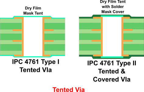
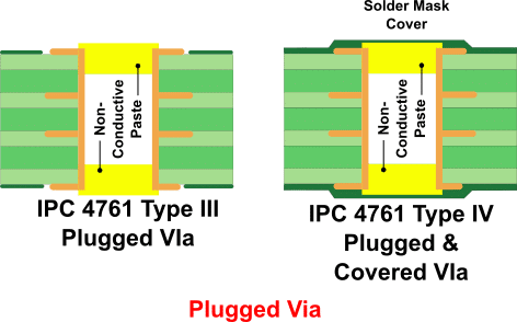
Plugged Vias: Plugging the via on one end or both ends with a non-conductive epoxy paste prevents solder flow-through or wicking during soldering. To allow the epoxy plug the hole effectively, Rush PCB limits the diameter of the via to a maximum of 20 mils. Fabricators often cover the plugged via with solder mask.
Filled Vias: Fabricators often fill a regular or encroached via with non-conductive epoxy paste. These filled vias have the solder mask stopping short of the pad by a few mils. This is a good compromise for medium density PCBs as the presence of the solder mask reduces the likelihood of solder bridging between the via and the neighboring pad.
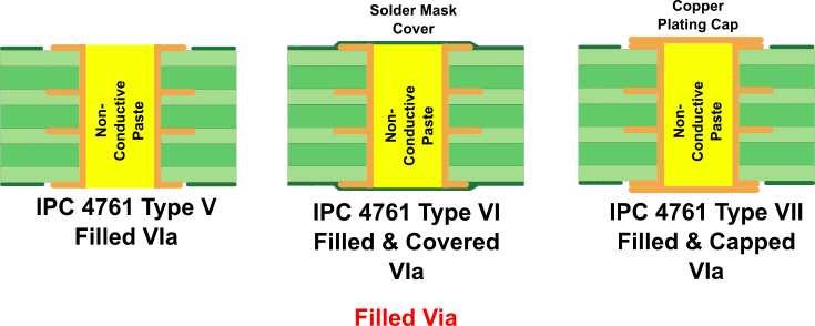
Rush PCB uses active pad processing, where a vacuuming process draws the non-conductive paste through the via hole, filling it entirely. We then planarize the ends, and cover it with solder mask.
For via-in-pads, where the via appears directly on the pads, we use active pad processing. However, instead of covering the ends with solder mask, we plate the surface with copper. This not only hides the via opening, but also makes the surface of the pad indistinguishable from other SMT pads that do not have a via underneath them.
Conductive Filled Vias: Rush PCB often fills micro-vias with a conductive paste to enhance their conductivity. This filling can be epoxy resin with copper, although sometimes we also use pure copper for the filling.
Conductive filling allows effective transfer of electrical signals from one side of the board to the other, while enhancing its thermal transfer properties as well. In fact, conductive filling is applicable to all other types of vias also.
Advantages of Conductive filled Vias
Copper filled micro-vias have several advantages. Some of them are:
- High Routing Density
- EMI Reduction
- Better Thermal and Electrical Conductivity
Being small, micro-vias allow high routing density on the PCB, allowing substantial reduction in overall PCB size and lower number of layers. All this reduces the cost of the PCB.
Rush PCB uses micro-vias for making their HDI boards with smaller form factor and lower weight. The lower form factor leads to a reduction in distances between components reducing the overall resistance of the tracks resulting in better electrical conductivity. The copper filling in the micro-vias further reduces the resistance of the vias. The higher conductivity helps in lowering EMI reduction as well.
With SMTs growing ever smaller, they need smaller pads for mounting them. As designers use via-in-pads for increasing the routing density, micro-vias are a good fit for the purpose, as regular vias are usually too large to fit inside small pads. This is especially true for breaking out connections for close pitch components such as BGAs.
Conductive filled vias are especially helpful for conducting a large amount of heat away from a hot component. The metallic nature of the fill wicks heat naturally away from the chip to the other side of the board for further dissipation by a heat sink.
However, there can be significant difference in the coefficient of thermal expansion or CTE between the metallic fill and the surrounding laminate. Metal heat up and expands far more rapidly than the laminate can. This unequal expansion can cause a fracture to appear between the pad and the hole wall.
Conclusion
Rush PCB has a huge expertise in manufacturing different types of PCBs for various applications. We make HDI boards for which micro-vias are an essential element. Depending on the application, we fill the vias with conductive or non-conductive paste. Filling the vias enhances the reliability of our boards.


