

With electronic equipment trending towards smaller and thinner form factors, engineers must use tiny Surface Mount Technology or SMT components on Printed Circuit Boards or PCBs. Most often, the board has a mix of fine pitch, medium-sized, and large SMT components. For effective assembly of such boards, Rush PCB recommends using step stencils.
What is a Stencil?
Assembling SMT components on a PCB requires depositing solder paste on pads on the board. The most optimum and accurate way of doing this is by using a stencil. A stencil is a thin sheet of steel with holes cut in it accurately matching pads on the PCB.
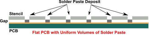
When an operator aligns the stencil on the PCB, he/she can squeeze solder paste through the holes in the stencil and deposit it on the pads on the board. To distribute the solder paste evenly, the operator uses a squeegee to pull the paste across the stencil. Once the operator lifts the stencil away from the board, some solder paste remains on the pads. The board with the solder paste then passes to the pick-and-place machine, which position appropriate SMT components on the solder paste. The populated boards then undergo soldering in reflow ovens.
Problems with Stencils
Thickness of the stencil and the area of the opening or aperture for a pad determines the volume of solder paste that the stencil deposits on the pad. The volume of solder paste on a pad is extremely important for proper soldering of a component. If the volume is low, soldering on the component may be inadequate. If the volume is high, excess solder may cause bridging with the neighboring pads. Rush PCB designs stencils with optimum aperture and thickness for effective solder deposit.
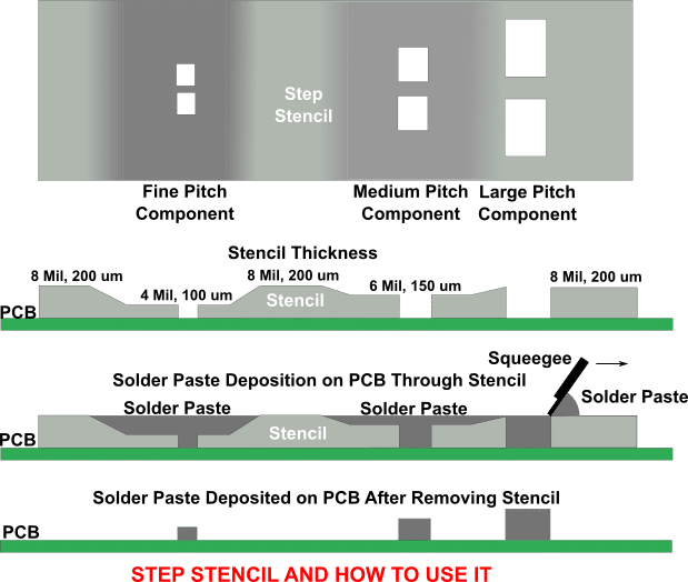
Even when the stencil has an optimum thickness and aperture, it may not be adequate for a board with a mix of SMT components with different footprints. For instance, ceramic BGAs need a high melting point during the soldering process, as the ceramic body absorbs a lot of heat and prevents solder balls from melting at normal reflow temperatures. For this, it is necessary to print higher volumes of solder paste on the CBGA pads, which requires a stencil thickness of 0.18-0.2 mm.
However, other SMT components like 0402 chip components and QFPs with 0.5 mm pitch or less need extremely small apertures on the stencil. Using such small apertures on a 0.2 mm thick stencil presents difficulties with paste release when the operator lifts the stencil—these apertures are best suit for 0.127 mm thick stencils.
Depositing solder paste effectively on a board that contains CBGA, QFP, and 0402 SMT components requires a step stencil—a combination of a basic 0.127 mm thick stencil with 0.2 mm thick areas for the CBGA. For good solder paste release, Rush PCB recommends final electropolishing for the stencil.
What is Step Stencil?
A step stencil essentially controls the volume of solder paste deposit on the PCB effectively for both large and small SMT components. Large SMT components require a higher volume of solder paste for good soldering, and a thick stencil is necessary. On the other hand, small SMT components do not need so much solder, and a thin stencil offers a better solution. A board with both small and large SMT components therefore, requires a step stencil—with thick areas for the large components and thin areas for small components.
Types of Step Stencil
Two types of step stencil are common—step-up and step-down.
Step-Up Stencil
PCBs with many small components and a few large SMT components use step-up stencils. The basic stencil is 0.1 mm thick steel sheet, with the thickness increasing to 0.15 mm for the large SMT components. The higher thickness forms a convex layer on the basic sheet, and remains flat on the side facing the PCB.

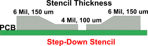
Step-Down Stencil
PCBs with many large components and a few small SMT components use step-down stencils. The basic stencil is 0.15 mm thick steel sheet, and the thickness reduces to 0.1 mm for the small SMT components. The lower thickness forms a concave layer on the basic sheet, and remains flat on the side facing the PCB.
It is possible to use step stencils with or without frames. Assemblers use framed step stencils for production runs, while frameless step stencils are more useful for prototype assembly. Frameless step stencils are less expensive than frame stencils are.
Fabricating Step Stencils
Manufacturers use one of three technologies for fabricating step stencils. They use:
- Photo-Chemical Etching Technology
- Micro-Machining Technology
- Laser-Welding Technology
Photo-Chemical Etching Technology: This is the primary method for fabricating step stencils. The fabricator applies a photographic process for applying resist on areas of the stencil that will not undergo etching. Then they spray an etchant onto the stencil surface to remove material until they achieve the desired thickness.
Micro-Machining Technology: The fabricator attaches the basic stencil sheet to a cooled vacuum plate on a milling machine. They use the CNC based milling machine to remove very small amounts of material at a time, until they have achieved the desired thickness. They mount the stepped foil on a frame and use a laser beam to cut the apertures.
Laser-Welding Technology: The fabricator uses two sheets—the basic thin sheet and a thicker sheet. They use CNC machines to cut out the area of the step from the basic thin sheet and the thicker sheet. They place the thicker foil cut out black into the cut-out area in the thin sheet and laser-weld the joint. The fabricators use laser beams to cut apertures.
Benefits of Step Stencils
Some of the benefits of using step stencils include:
- Optimum solder paste volume control
- Eliminating multiple print processes
- Replacement for several single stencils
- Can solve problems of gasketing, solder shorts, and paste smearing
- Possibility of steps on the squeegee side and relief on board side of same stencil
Conclusion
Rush PCB has the technical ability to fabricate step stencils in both single and dual processes. Complex PCBs require different solder paste volumes for various SMT components. Using various foil thicknesses on the same stencil helps to deposit adequate solder on coarse pitch areas while accurately controlling solder paste deposit in fine pitch areas.


