


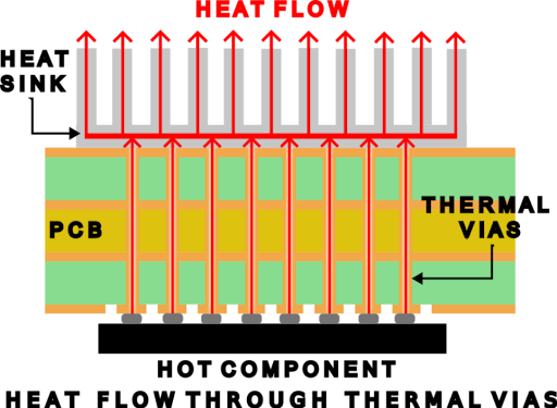
Thermal vias are used at Rush PCB to move heat from one layer to another within a multi-layer PCB. These are special vias near thermal generating components to move heat away from that component and reduce the chance of overheating. Thermal vias are often used in conjunction with copper planes, thermal pads and heat sinks. A thermal via is simply a PTH which is positioned underneath the thermal generating SMD component. To get to grips with thermal vias you must also understand how the thermal path works.
Thermal Path
Heat created in the component die travels through exposed copper pads, through thermal via arrays to a copper plane or metal core. At times, a heat-sink is used to increase the surface area for thermal dissipation to ambient.
Why use Thermal Vias?
Thermal vias are used to lower thermal resistance by transferring the heat generated from a hot component on the component side of the PCB to a copper plane on the opposite layer or to a metal core. If a heat sink is attached to the copper plane or metal core then thermal vias will be beneficial. Thermal vias are required if the following applies:
- The junction temperature of the hot component may be over the safe operating limit.
- The power device is dissipating 1 watt or more.
- Power devices are QFN, DFN, to-220 or power-MOSFET packages with exposed metal pads.
- Thermal vias are required on the following types of PCBs: LED, DC-DC, RF Amplifier and BMS/Battery Management.
Thermal Via Design Rules
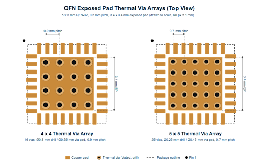
We recommend using multiple smaller vias rather than a few larger ones. We recommend 0.3mm finished hole size and 1.0-1.2mm hole spacing. Thermal vias must be directly underneath the exposed pads.
| Parameter | Recommended Best Practice |
| Via Dia | ~0.3mm for good plating |
| Pitch | Start with 1.0-1.2mm pitch. |
| Array Size | Most QFN/DFN pads should use between 9-25 thermal vias. High power targets may require between 16-25. |
| Fill | Best thermal performance will be achieved with copper filled vias. To prevent solder wicking use epoxy filled vias with copper capping. |
| Connection | Use vias to connect to one large copper pour, and if needed a heat sink. Do not connect to an isolated copper island. |
Thermal Via Placement
Where you place your thermal vias can be just as important as having the right number. So here are some tips:
- Ensure your thermal array is positioned directly underneath the thermal pad of the hot component.
- The large copper pour must be much larger than the footprint of the hot component.
- Do not use open vias underneath small solderable pads. The solder will wick away during reflow.
Special Cases
Metal-Core PCBs
Thermal vias on metal-core PCBs are also PTHs. The vias are placed in specific areas to transfer heat from the hot component on the top copper layer through the insulation dielectic layer to the highly conducting Copper/Aluminium base. Unlike signal vias, the focus for thermal vias is the thermal performance, with copper plating and conductive fill to reduce thermal impedance.
Metal-core PCBs will typically have a core with a thermal conductivity of ~200 times greater than an FR-4 material on standard PCBs. For thermal vias to work they must be placed to transfer the heat generated by the component to the core. This creates multiple parallel paths with low thermal impedance reducing the overall thermal resistance of the PCB.
Adding thermal vias ensures reliable operation of high power electronics by ensuring you improve the performance of the PCB. If you do not use thermal vias the heat will become trapped around the component increasing the junction temperature, reducing efficiency and causing failure in demanding environments.
Design Rules for Metal-Core PCBs
When designing your thermal vias you should take the following into account:
1. Dielectric Layer
Insulation between the copper circuit and metal core. This is usually non-conductive and will be a major source of thermal resistance.
2. Thermal Pad Copper Areas
You should not solely rely on thermal vias. Try to maximise the amount of Copper underneath the MOSFET, LED or regulator.
3. Via Usage on MCPCBs
If the hot component is situated directly on top of a good metal core (with minimal dielectic thickness) then you may not require thermal vias. If you need the heat to travel through multiple layers then you may require thermal vias.
4. Mounting Interface
The following can contribute greatly to thermal performance:
- Thermal grease.
- Thermal pads.
- Tightening of screws.
- Flatness between heatsink and MCPCB.
Useful Tips
- Using between 16-25 thermal vias will significantly reduce the thermal resistance compared to 4.
- If you are using low power or small hotspots 3×3 or 4×4 arrays directly underneath could be sufficient.
- Medium power will benefit from a higher density array of filled vias and solid copper pours on multiple layers.
- Very high power can benefit from using more vias, thicker copper, exposed copper pads, multiple thermal planes and heat sinks. You may also want to use heavy copper or MCPCBs.
Common Mistakes
- Only using a few large vias.
- Connecting to small isolated copper islands.
- Only relying on thermal relief on planes where maximum thermal performance is required.
- Not considering the effect of the dielectic layer on MCPCBs.
- Not considering solder wicking on via-in-pad designs.
- Assuming more via will make up for poor heat sink or airflow design.
- Not using thermal simulation or testing for temperature on your prototype.
Thermal Via Checklist
- Identify all components generating significant power.
- Place thermal vias directly underneath all exposed pads of the hot components.
- Use many small vias with a tight pitch.
- Fill or cap vias if solderability is required.
- Ensure all vias are connected to large continuous copper.
- Ensure copper extends beyond the package size and into the heat sinking area.
- Consider using MCPCB, heavy copper, thicker planes or active cooling for extreme power.
- Validate with thermal simulation and junction/case temperatures.
Conclusion
At Rush PCB we understand thermal vias are just part of the thermal chain. Our best high power designs utilise via arrays, copper areas, stackup selection, metal-core construction where applicable and a reliable connection to a heat sink or airflow.
FAQ
Q1. Can thermal vias help on a single layer aluminium metal-core board?
A1. Usually no. The heat only has to pass through one insulation layer to get into the metal base which will spread it. Via arrays on FR-4 boards will not help.
Q2. What stops heat passing through my metal-core board and how can I improve it?
A2. MCPCBs have a very thin insulation layer between the copper and metal base. This will typically be between 50-150µm thick and have a thermal conductivity of between 1-3W/m.K. If you can use a thinner insulation layer with a higher conductivity you will be able to pass more heat through but you need to consider your voltage requirements. As a rule of thumb 75µm will be sufficient for low voltage circuits (<60V). Mains circuits (>250V) will require 150µm or more (tested for 4kV).
Q3. Can I route a via straight down to the metal-core?
A3. A standard metal-core board will not have any through-holes into the metal core. Some fabricators can provide a “direct thermal path” by removing the insulation underneath the thermal pad. This will mean that the pad is almost directly on the metal. The pad will have little or no electrical isolation from the metal core. However this can only be used on pads which are not electrically connected, or are the same voltage as the core.
Q4. When should I use thermal vias on my metal-core board?
A4. If you have a multi-layer MCPCB then you will need thermal vias to transfer the heat through more than one insulation layer. As a starting point use 0.3-0.5mm holes with 1.0-1.5mm spacing and 35-70µm plating. Try to fit as many vias as possible underneath the pad of the power device.
Q5. What via layout should I use on high power GaN/SiC parts on FR-4 boards?
A5. A common via layout is 0.3mm holes with 0.6mm pads and 1.0-1.2mm spacing. Be aware that if you have tighter spacing it can affect the integrity of the board. Use copper filled, flattened vias with plating over underneath exposed pads. This will prevent solder wicking into the holes during reflow.
Q6. When should I stop adding vias and use a copper coin instead?
A6. If the additional vias are giving less benefit due to the board material becoming a bigger factor.
- Typically a copper coin (solid copper slug pushed into the board) will give approx 0.5-2°C/W compared to around 5-15°C/W for a via array.
- As a rule of thumb you will need a coin if a small area is dissipating more than around 10-20W.
- Example: On a 1.6mm board a 2mm coin will give approx 1.3°C/W. This would require around 145 vias with 0.3mm holes to match.


