

The design of every Printed Circuit Board (PCB) is unique. Each PCB has its own requirements, and individual trade-offs on its design. Rush PCB recommends using basic guidelines for component placement on PCBs that turn the design into a professional endeavor making transition from design to production an easy process.
According to Rush PCB, one of the basic concepts of component placement during design is grouping components according to their functional performance. Grouping them into functional blocks has advantages of keeping things organized and allowing easier tracking of signals. Additionally, it helps keeping the average track length short, leading to a better control on reflection and cross-talk. Another advantage of such grouping is it provides an estimate of the space the circuit needs, and leads to a good approximation of the overall size of the board. Changes to the design can alter the board size and therefore, designers always maintain some loose constraints, filling the available space by expanding the placement. Some other concepts of proper component placement and ease assembly are:
Shadow Effect
During reflow, larger SMD components tend to throw a shadow over their smaller counterparts, if the spacing between the two is small. This shadow effect partially prevents hot air or IR radiation from reaching the smaller parts, which do not heat up properly, resulting in poor quality soldering of the smaller components.
Rush PCB recommends avoiding the shadowing effect by misaligning the component placement using a combination of staggering pads. As this avoids placing the components directly behind one another, the IR heat reaches all components in equal proportions.
Rush PCB also recommends increasing the spacing between the components, as the effect of the shadow of the larger component reduces with increasing distance. Designers prefer to maintain a minimum of 25 mil spacing between components, but allow the spacing to increase to 100 mil to avoid shadowing.
Also Read; Factors Affecting the Longevity of Copper Bond
Shadow effect is more prevalent with wave soldering, as the technology requires a larger spacing between components to avoid solder bridging. The general rule of thumb designers follow is using double the spacing they would keep when designing for reflow soldering.
Smaller infrared ovens also have this problem, especially where the board remains immobile, and a small source generates the infrared heat. As the heat rays fall at an angle on the board, smaller parts are likely to come under the shadow of larger ones. Designers must be careful to not place smaller components close to larger ones to avoid the shadow effect. However, this challenge may not be present in ovens using a more uniform method of heating.
Thermal Load and Component Size
For boards with components on both sides, it is important for the designer to balance the thermal load. Larger components have higher thermal mass, requiring more time, or a higher temperature profile, to reach the solidus temperature than smaller components require as they have a smaller thermal mass.
Reflow machines subject both sides of the board to the same condition with a single thermal profile. If the board has a concentration of large and heavy components on one side and small and lighter components on the other, the thermal profile will suit only one of them. Optimizing the thermal profile for the side with smaller components will leave the side with the larger components improperly soldered, as they would not have reached the necessary temperature for proper soldering. On the other hand, optimizing the thermal profile for the side with larger components would subject the other side with damaging levels of heat. Designers must take care to intermix the two sizes to effectively keep the thermal load in balance.
Boards with SMDs undergoing wave soldering need a drop of glue to attach the components to the PCB surface and prevent them from falling off. With decreasing size of the component, the amount of glue dispensed must also reduce to prevent the glue spreading on to the pads. Surface underneath small SMDs such as 0201 or 01005 are not adequate for accurate glue placement. Although for high frequency boards and or physically small boards designers prefer using small SMDs, they should rather use components larger than 0805, especially if the board will undergo wave soldering.
Polarized Components
Randomly orienting polarized components on a board increases the opportunities for mistakes, both during assembly, and during testing. A better practice is to align all polarized components in the same direction, along the X- or Y-axis. For instance, designers must place diodes, LEDs, and polarized capacitors with their anodes in a specific direction, and cathodes in the other. To help the pcb assemblers, designers may implement this information in the copper layer provided space permits, or else, in the silk screen.
Proper labeling of every polarized component is extremely important whether the board is to for manually assembly or machine population. Unclear labeling of polarized components may lead to human error or an incorrect programming of the pick-and-place machine. Either way, this can be an expensive mistake for high volume production.
Uniform Pads
Pads on both sides of a two-terminal SMD must be identical. This helps to equalize the forces liquid solder exerts on the component during reflow. Unequal forces as a result of non-uniform pads allows more solder on one side of the component, which, as the solder melts and moves to cover the terminal, exerts a greater force on the component, pulling it towards the pad. As the other side has less solder and exerts a lower force, the component lifts and stands straight up on its side. The vertically standing component looks like a tombstone, and engineers call this effect tombstoning.
Thieving Pads
Boards with closely packed SMD components and high pin count devices must deal with bridging during wave soldering. Component skewing and tombstoning are not a factor here, as the glue between the SMDs and the board makes the parts immovable. Bridging is more common on a long row of leads in the direction of board flow. As the solder flows over the pads, each pad draws the solder away from its preceding pad, allowing just the right amount of solder to remain.
However, at the last pad, there is no other to pull the solder along, and it the collects in a ball, creating a solder bridge between the last two leads. Engineers circumvent this problem by creating a thieving pad—a larger pad on the trailing lead of the device. The larger surface area of the thieving pad wicks the excess solder from the last lead, pulling it away before it can create the bridge.
Design of the Board
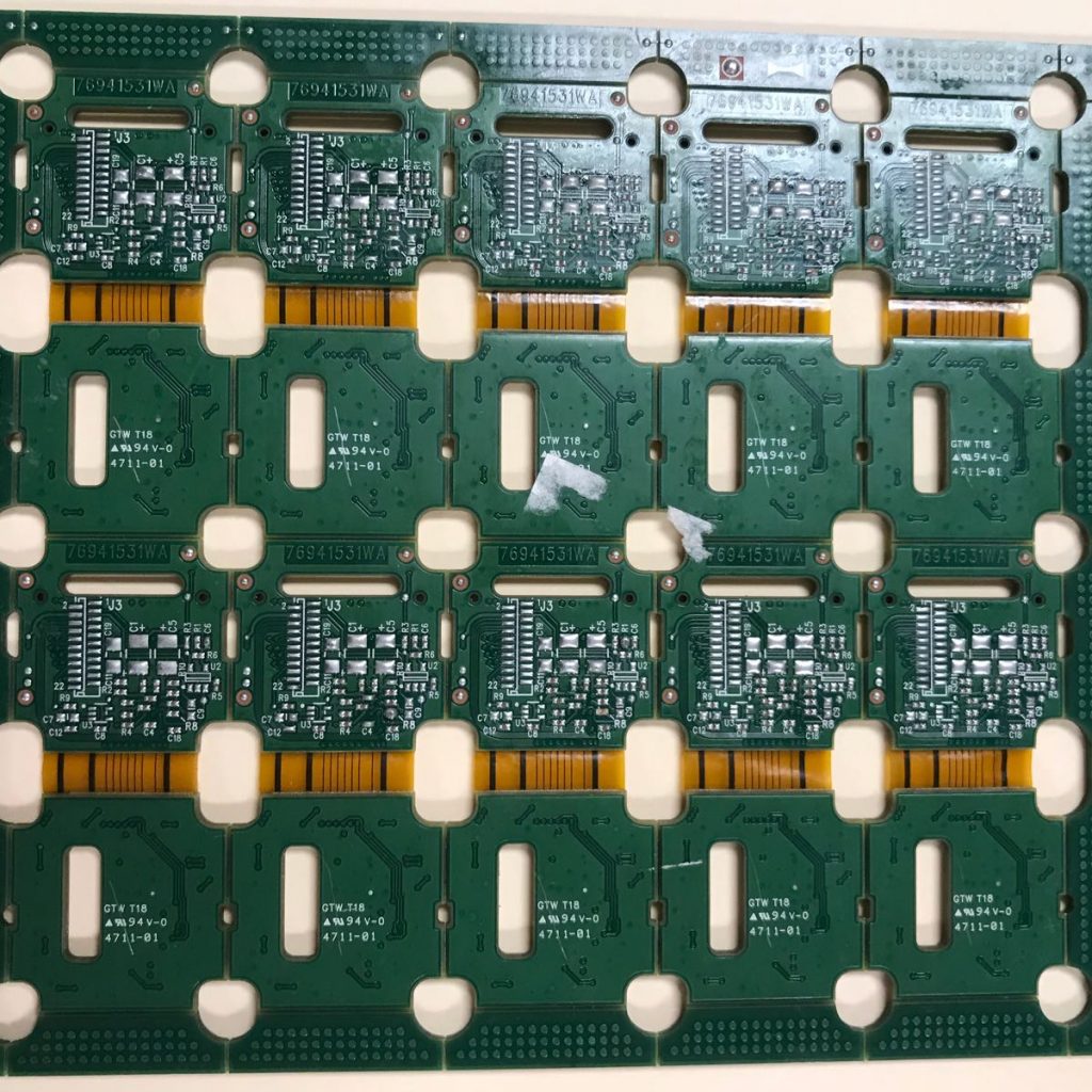
Although the project defines the ultimate shape of the board, odd shapes make assembly with automatic equipment difficult. Automated assembly requires the machine to grip the board to either keep it steady or move it in a controlled manner. For this, the board must have at least two parallel edges.
For odd shaped boards, manufacturers prefer to leave the board connected to their larger panels during the assembly sequence. They provide mechanisms to separate the board after assembly, and these mechanisms can be either V-grooves or a series of perforations (rat bites).
Designers must be careful when providing the area for gripping the board, as overhanging parts such as audio connectors and USB ports are likely to interfere with the grip. Making a special grip to accommodate the overhanging part is usually an expensive proposition, and repositioning the overhang to include it elsewhere on the PCB might be more worthwhile.
Inclusion of Tooling Holes
The manufacturing and assembly processes make use of several tools mostly for referencing purposes. For instance, tooling holes in PCB laminates allow the operator to stack them quickly and accurately on top of each other for drilling. The same tooling holes allow operators to position the PCB properly when dispensing solder paste, and again, for positioning the board in pick-and-place machines for mounting SMDs. Pick-and-place machines also use special tooling holes as fiducials when mounting large fine-pitched components.
Electrical testing jigs can also use these tooling holes to orient and position the board properly. Additionally, the product enclosure may also use these holes for mounting the board in place. As tooling holes have multipurpose uses, engineers use them in standardized sizes. They also do not plate tooling holes, as the uncontrolled thickness of the plating process could cause the hole diameter to vary.
Conclusion
Although Rush PCB does not guarantee that all the steps discussed above will always result in perfect results, a well-designed board with properly placed components is likely to yield better results rather than an adequately designed board. Designers will need to balance the benefits and drawbacks of each step before they apply, and with experience, introduce them within the design methodology, resulting in higher quality of circuit boards.


