

In part 1 of this article, we covered how panelization can save both time and material through the fabrication and assembly of multiple PCBs in the panel at the same time. The higher the number of PCBs we can accommodate in a panel (after consultation of Fab and the Assembly house), the higher are our gains in terms of both time and money. At Rush PCB Inc., we utilize panelization as a tool to enhance the overall production efficiency by improving the quality and reliability of the final product. We start things keeping in view how we are going to end it. We essentially panelize multiple PCBs into the panel, knowing that at the end, we have to separate them back to single PCBs. This process is called De-Tabbing. In this article, we will be covering what de-tabbing is, what its different types are, how to define those in the panels, and how to select one in our panel.
How to separate the individual PCBs from the panels?
Once the PCB panels are fabricated and components are assembled on them, the next important step is to separate the individual PCBs from the panels. This process is called De-Tabbing. We will cover its details and types in Part 2.
De-tabbing Options
De-tabbing refers to the process of separating individual PCBs from a panel after assembly. The method chosen depends on the board design, production volume, and edge quality requirements. Below are common de-tabbing options:
- Route & retain with mouse bite holes
- Route & retain with solid tabs
- V-Scoring
Route & Retain with Mouse Bites (Perforated Tabs)
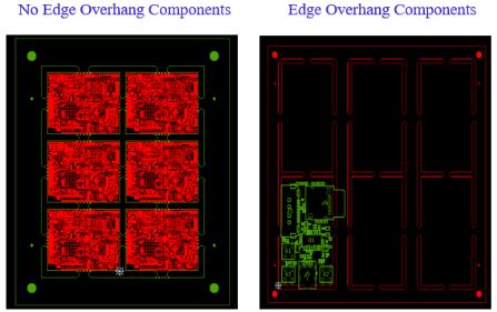
Small drill holes create a breakaway point, easy to snap off manually or with a fixture. After deburring, it leaves a slightly rough edge. If your PCB design has an irregular shape, tab routing may be required for panelization. For standard designs, we maintain a 2 mm (78.74 mil) spacing between adjacent boards in the panel to allow for proper routing and separation. However, if edge components (such as connectors) extend beyond the board outline, we must increase the spacing between boards to compensate for the overhang. For example, if an edge component extends 300 mil outside the board edge, we maintain a 400 mil distance between the two adjacent boards in an array. This additional spacing ensures easier de-tabbing and protects edge-mounted components during separation. Refer to the images below for examples of both standard and edge-component situations.
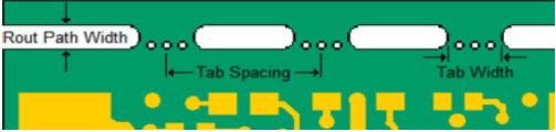
Consider the following requirements when using route & retain with mouse bite hole depanelization method.
| Parameter | Specification |
| Route path width | 0.078 INCH |
| Tab width | 0.2 INCH |
| Tab Spacing | 2.0 INCH max (center to center) (Corner to first tab within 0.5 INCH) |
Key Points:
- Avoid using on PCBs thicker than 0.093″ (2.3622mm)
- Joint strength using drilled breakaway routing is weaker than solid tab routing
- Depanelization is by manual methods (hand, nibblers, plyers)
- Routed areas are smooth with some exposed fiber at tabs, leaving approx. +/-0.005″ (0.1270mm) of material residue
- Tabs should be positioned 0.078” away from edge components to avoid any damage to the component during de-tabbing
Route & Retain with Solid Tabs
In the Route and Retain with Solid Tabs method, the individual PCBs are fully routed (cut) along their outlines, leaving solid tabs at certain points to hold the boards together within the panel during manufacturing and assembly. Since these tabs are unperforated hence provide greater panel strength during assembly, reducing flexing or warping.
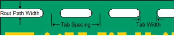
Consider the following solid tab routing requirements when using the solid tab depanelization method.
| Parameter | Specification |
| Route path width | 0.078 INCH |
| Tab width | 0.1 INCH |
| Tab Spacing | 2 INCH max (center to center) (Corner to first tab within 0.5 INCH) |
Key Points:
- The joint strength provided by solid tab routing is significantly higher than that of V-score or drilled breakaway (mouse bite) depanelization methods
- Depanelization may only be performed with a machine, either a high speed automated router or shearing machine.
- Routed areas are smooth, leaving < 0.005″ (0.1270mm) of material residue.
- Tabs should be positioned 0.078” away from edge components to avoid any damage to the component during de-tabbing. It may involve part height considerations as well depending upon the type to tooling being used for the de-tabbing purpose.
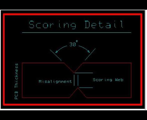
V-Scoring
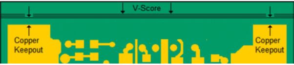
At Rush PCB Inc., we also use V-Scoring (also called V-grooving) as a depanelization method where shallow grooves are cut into the top and bottom surfaces of the PCB along a straight line. These grooves are typically cut about one-third of the way through the board thickness on each side, leaving a thin web of material (about 1/3 thickness) that holds the boards together during assembly.
Consider the following requirements when using the v-groove depanelization method.
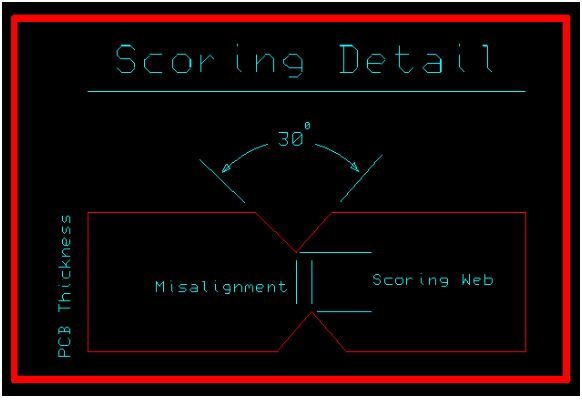
| Parameter | Specification |
| Angle | 30 Degree |
| PCB Thickness | Preferred for 0.062” to 0.093 |
| Max Top to Bottom Misalignment | 0.004” |
| Web Thickness | 0.014” +/-0.002 “ |
Key Points:
- Joint strength using V-score is weaker than solid tab routing and may be more susceptible to handling issues especially for larger panel sizes.
- Depanelization may be performed manually or with a machine
- Scoring provides a uniform but comparatively rough edge 0.004” to 0.010” of residue material
- If edge component placement allows, the boards may be placed adjacent to each other.
De-tabbing Equipment:
Even if your PCB array is designed well, problems can still happen when breaking the boards apart. If it’s not done the right way, the board can splinter, tear, or damage components. That’s why it’s important to use proper de-tabbing methods and tools to avoid extra costs.
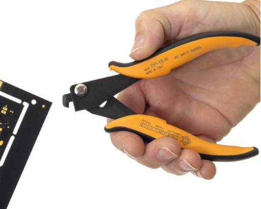
Pliers & Nibblers
A well-designed tab-routed PCB panel can often be broken apart using hand tools. For best results, use wide-nose pliers to bend each tab along the break line until you hear it crack. Then, bend the tabs the other way to completely separate the boards. This de-tabbing method can be used mostly for the tabs having mouse bite holes.
Second Route Operation
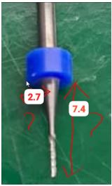
Another way to separate PCBs from rails or each other is by using a high-speed routing machine. As shown in the picture below, this method uses a router bit and requires careful attention to the size of nearby components. If a part is placed close to a solid tab, its height and width must not exceed 7.4 mm and 2.4 mm. Otherwise, the secondary routing process could damage the part. We carefully take all of these factors into account when designing array drawings.
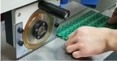
Pizza Type Auto/Manual PCB Cutter
This method uses a newly designed linear or circular cutter that completes the micro shear-stress cutting stroke in a single motion. It’s suitable for all types of tabs. During the process, the PCB remains stationary while the cutting blade moves back and forth. This helps minimize shear stress and reduces the risk of product quality issues. The cutting machine is made of high-speed steel, making it durable and reusable
However complex your PCB may be, you can rest assured that we, at Rush PCB Inc., will fabricate it for you. Contact us today for your instant quote.


