

Rush PCB designs PCB panels or arrays such that the constituent smaller PCBs remain securely attached during manufacturing and assembly. However, our design also allows easy depanelization into individual boards for shipping to our customers.
PCB panelization involves bringing together several smaller individual PCBs to form a large panel, usually of standard dimensions. This helps in mass production or quick turn PCB assembly as it optimizes output. At Rush PCB, we find the best way to arrange and fit individual printed boards in a large standard blank to use in our manufacturing process.
Fabricating and assembling one large PCB panel offers a higher throughput compared to handling several smaller individual boards. Placement machines must stop several times in between when populating several smaller boards to allow changeover, When the boards are in a panel, this changeover time is not necessary and the placement machines can function continuously.
PCB Panelization Considerations
While designing for panelization, it is also necessary to consider the process of PCB assembly as well, including handling by the placement machinery, and the conveyor carrying the assembly through the reflow oven. Typically, machinery throughout the assembly process needs the panel to have tooling strips on at least two opposite sides. Tooling strips help secure and stabilize the PCB without disturbing the components onboard.
Apart from handling, other considerations need addressing, and these include:
Panel Size: Maximum size of the panel that processing machinery can handle.
Fiducial Marks: These marks allow vision alignment in different machines to achieve a high level of accuracy for locating the components with respect to the PCB. The standard practice is to add three fiducial marks to three corners of the panel to allow the machine to check proper loading of the PCB. High density, close pitch components require higher accuracy while placement, and designers achieve this by placing additional fiducial marks on opposite sides of the copper pattern on the PCB.
Tooling Holes: Not all machines have vision alignment, and these machines use tooling holes in the handling edges or tooling strips for proper alignment of PCBs while processing them. Typically, two tooling holes along one tooling strip is adequate.
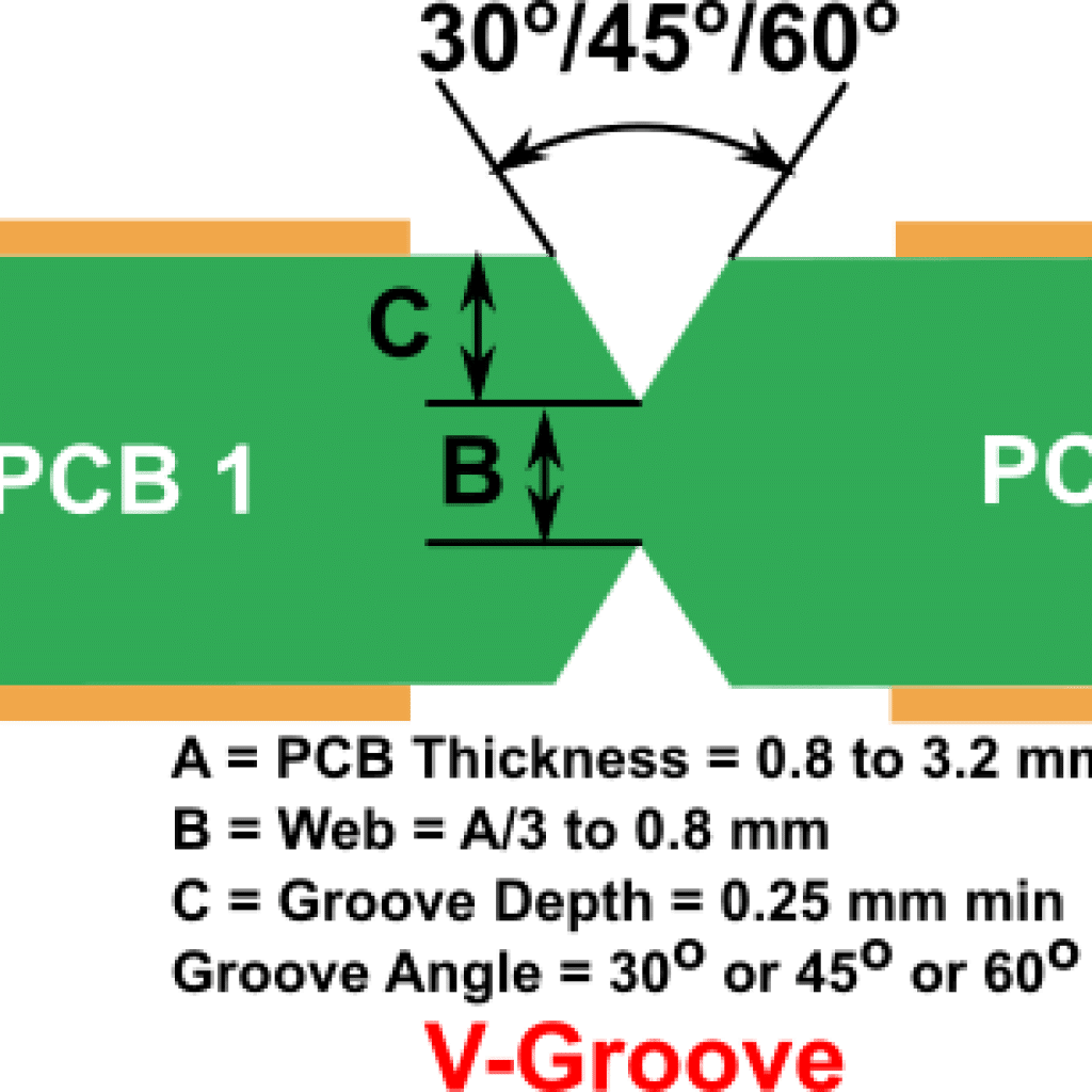
Depanelization: This is the method the assembler uses to separate individual PCBs from the panel after completing the assembly process. The depanelization method may use a manual process using simple hand tools. The designer usually weakens the parting line using either a v-scoring method or by using tab routing.
V-Scoring: The fabricator uses a machine to cut a deep v-groove along the parting line on both sides of the PCB, leaving the PCB connected by a thin web. When depanelizing, the operator uses a hand tool to bend the waste part of the PCB to break the web off along the groove. V-scoring works best for PCBs with thickness of 0.8 mm or more.
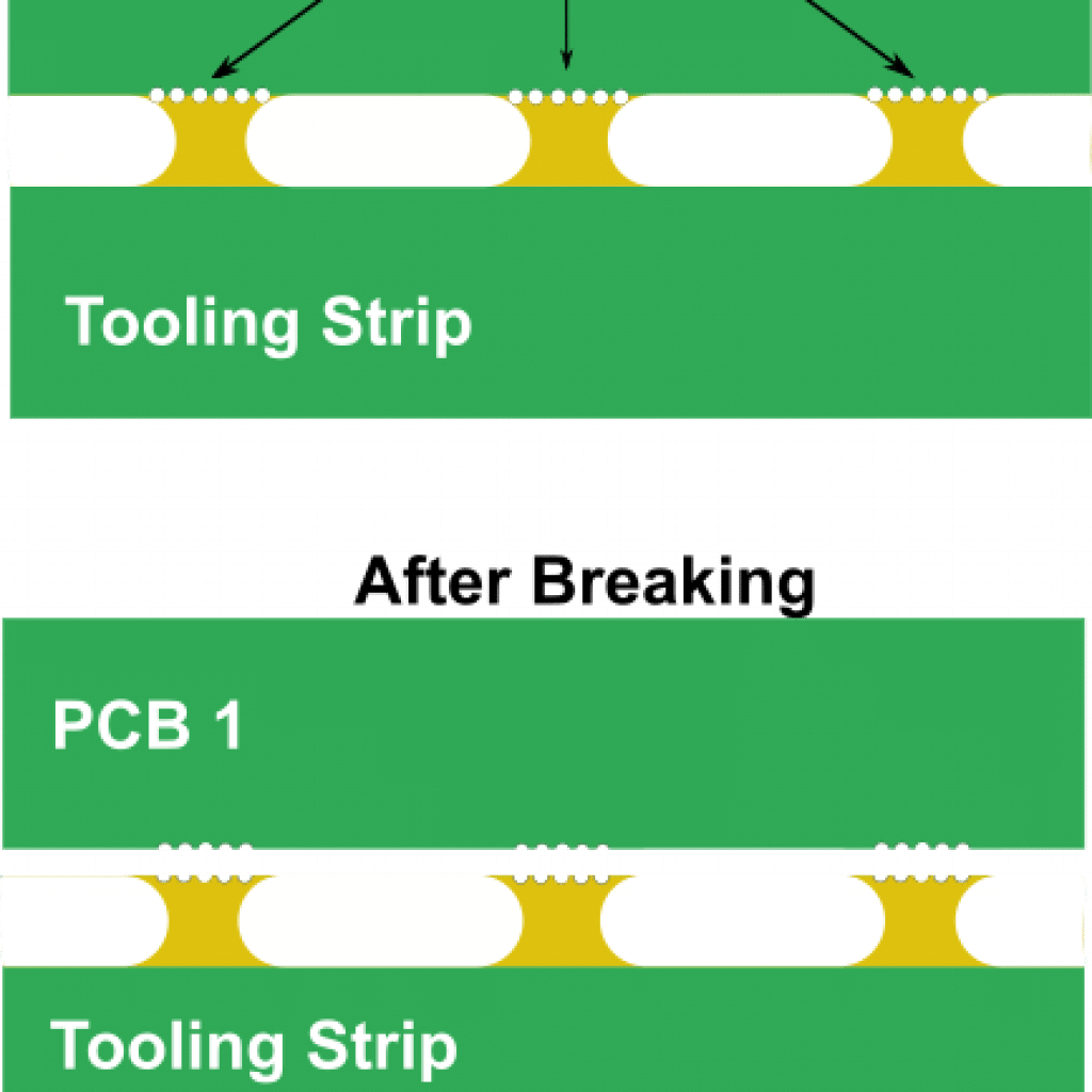
Tab-Routing: The fabricator uses slots to separate the PCB and the tooling strip, leaving them attached through mouse-bites. Mouse-bites have a series of holes to help the operator break out the PCB when depaneling.
PCB Panelization Types
Before starting the panelization process, Rush PCB confirms the design of individual PCBs through exercises such as Design for Manufacturing or DFM and Design for Assembly or DFA. The final panel must also conform to our manufacturing capabilities of automated equipment such as paste printers, SMT machines, reflow ovens, AOI equipment, and others.
We use several methods of combining PCBs for creating a panel. These are:
Ordered Panelization This is a method we use commonly as it offers several advantages. Ordered panelization is compatible with almost all types of PCBs, and not much consideration is necessary for SMT assembly conditions and product combinations.
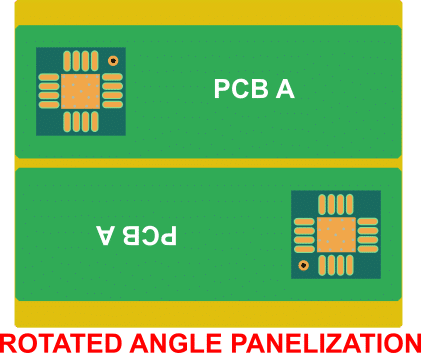
Although it achieves optimum material utilization, rotated angle panelization features some disadvantages. As heads in mounting machines must often rotate while placing components, the mounting efficiency decreases. Some mounting quality also suffers due to frequent rotation of the heads.
As the PCB pattern frequently changes, visual inspection is slower, as the operator must adjust to a direction change while inspecting a panel. This may lead to lower efficiency of inspection.
Combination Panelization
We use combination panelization when panelizing different types of PCBs. Combination panelization is especially beneficial when manufacturing different PCB types at the same time.
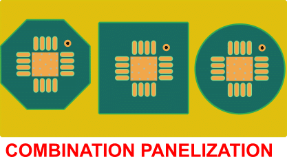
Combination panelization improves production efficiency while reducing costs drastically. However, combination panelization has many disadvantages. Major among them being the difficulty in handling product differentiation. Combination panelization also makes it difficult to analyze quality issues during assembly.
Deciding the Most Optimum Panelization Method
At Rush PCB, we decide the most optimum panelization method to use based on the improvements in manufacturing efficiency and reduction in difficulties and cost. While designing the panel, we must also consider the deformation forces that can produce PCB warpage during reflow.
We decide the most suitable depanelizing method to use based on the PCB thickness. For PCBs above 0.8 mm, we prefer to use v-grooves. For thinner PCBs we prefer to use tab routing. However, the presence of force-sensitive components on the PCB also affects the choice of depanelization method.


