

The latest development in fabricating PCBs is following the same trend that integrated circuit manufacturers are. They are packing increasing amounts of functionality into smaller spaces. However, the smaller the spacing is, greater is the difficulty in making precise manufacturing, as high-density PCB design requires following strict DFM rules.
Currently, Rush PCB is following three key processes as the latest game-changers in the design and fabrication of HDI boards:
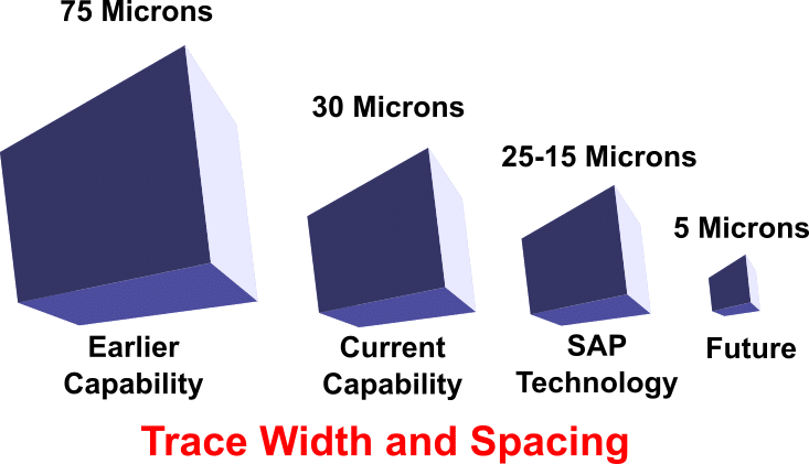
- Semi-Additive Process for achieving 1 mil (25.4 microns) trace widths and spacing
- Flexible design for IoT PCBs
- Advanced routing for DDR memory
Semi-Additive Process for Achieving 1 mil (25.4 microns) Trace Widths and Spacing
Traditionally, as fabricators, we use a subtractive process for creating circuit patterns on PCBs. Starting with a copper-clad laminate, a series of process steps removes unwanted copper, leaving only the intended circuit pattern. However, the traditional subtractive process can achieve a 3-mil (76.2 microns) trace width and spacing at its best.
With the semi-additive process, we begin by completely stripping the copper layer from the copper clad using an etching process, and adding a very thin layer of electroless copper on the base dielectric material. We then process this copper by imaging with the intended circuit pattern, and adding electrolytic copper to add on to the pattern.
The main advantage of the additive process is it allows achievement of feature sizes much smaller than the subtractive etching can. This is due to elimination of the trapezoidal effect the etching process has on the copper track.
After creating the circuit pattern, we proceed to process the PCB layer in much the same way as for a typical PCB layer. The semi-additive process integrates seamlessly with the imaging and chemical processes that we are already utilizing for subtractive etching. This helps not only to bring the process in-house, but also reduces our capital expenditure.
There are several advantages of the Semi-Additive Process:
- Reduction in the total number of layers necessary for routing
- Reduction in PCB space
- Reduction in PCB thickness and weight
- Useful for smaller packaging
Flexible Design of IoT Devices
Increasing requirements from IoT devices are forcing PCB designers to fit more and more circuitry into smaller spaces. For instance, a smart watch requires a display, battery, and sensors that take up most of the space. In addition, the smart watch also requires circuitry for CPU, memory, graphics processing, and wireless capability.
Rush PCB makes IoT designs smaller, lighter, and faster by working more with advanced design technologies. These include the High-Density Interconnect or HDI technologies, embedded components, and compact components like three-dimensional ICs and multi-chip modules. Additionally, all this requires using flex PCBs as a crucial component for the design of IoT devices.
Rather than use standard PCBs, we build the sensor and the PCB components onto one flex PCB. Not only does this minimize the requirement for several individual boards for the ioT device, it allows the circuit to fold and fit precisely into the device.
There are several advantages of using flex PCBs with HDI technology for IoT devices:
- Substantial improvement in performance and reliability
- Substantial improvement in signal quality
- Reduction in power consumption
- Lowering of thermal stress
- More robust design
- One PCB for the entire circuitry
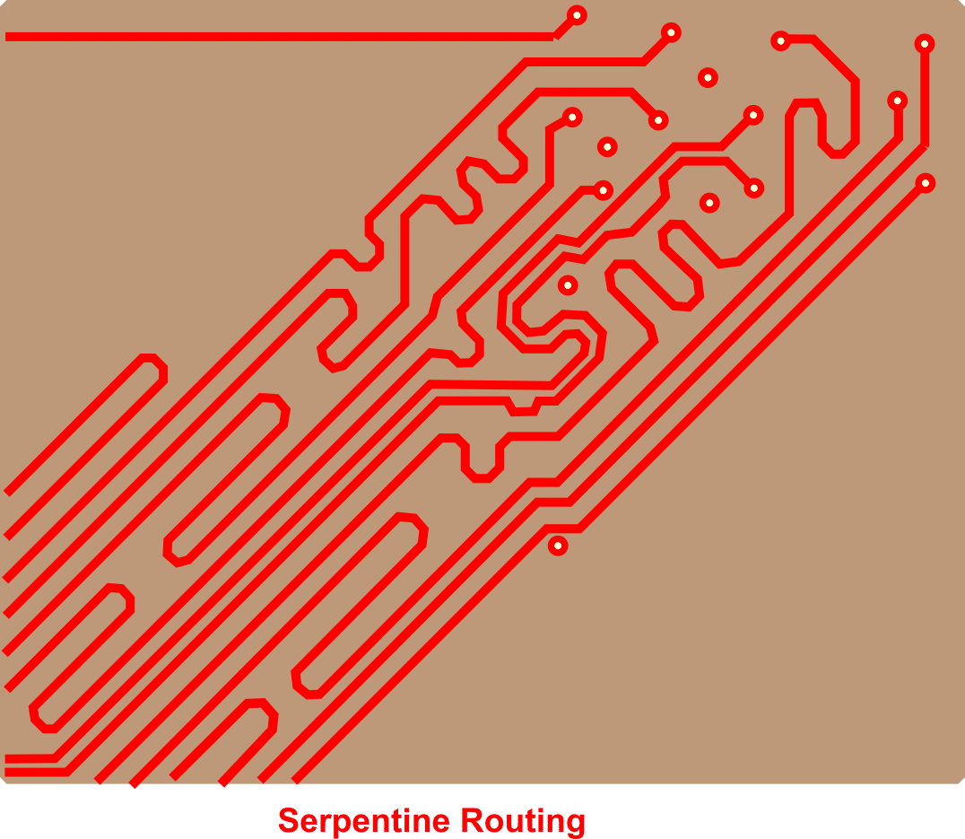
Advanced Routing for DDR Memory
Smart device with advanced computing powers are in use every day. People are regularly using smartphones, computers, wearables, and automotive systems requiring high speed processing. All these need the high-speed DDR memory to function. With the introduction of DDR5, the devices are entering a new standard of performance.
Complications arise in PCB design for DDR memory because of the need for individual signals to meet timing specifications. Timing of individual signals is important, so that the memory captures the data on the rising and falling edges of the associated clock line. While it is not possible to speed up electrical signals, the only way to control the timing is to slow down the signals so all of them arrive simultaneously at the appropriate manner.
Rush PCB uses serpentine routing to add length to the traces of signals for controlling their timing. Additionally, there are other requirements. Traces on the internal layers of the board will have different timing characteristics compared to those routed on the external layers. This is because ground planes enclose the internal layers, while the external layer has only a single plane adjacent to it.
Therefore, routing on the external layers follow the microstrip configuration, while those on the internal layers follow stripline configuration, as the latter remains sandwiched between two planes. With the introduction of each new version of DDR memory, the precision in routing becomes even tighter.
We begin DDR routing with the BGA escape routing and matching the termination in the transmission lines. Rather than a simple matter of hooking up traces, DDR routing requires careful planning starting from the initial escape routing and continuing all the way through to the end.
Although some traces may be short, they add up to some delay in the high-speed digital lines, causing problems of reflection. Unless we terminate the traces properly, voltage waves propagate down the line and collide with the waves of the original signal. The result is either a cancellation of the original signal, or adding to it, depending on the polarity of the two colliding waves.
Requirements for Successful DDR Memory Routing:
- Component placement must be optimal
- A routing plan is necessary
- Older DDR memories work better with T-topology
- Newer DDR memories require fly-by topology along with daisy chain patterns
- Advanced PCB Design software tools
Conclusion Rush PCB is a recognized PCB manufacturer with over 20 years of experience in this industry. Our expertise is in all types of rigid, flex, rigid-flex, and quick-turn projects. Our business is famous for its same day response, and we can fulfil projects with unique specifications of lead time, volume, and technology.


