

While at Rush PCB we manufacture and assemble various types of printed circuit boards (PCBs) for our customers, we also recommend professional and timely inspections for preventing failure issues. On the PCB side inspections can weed out failure issues such as due to delamination, cracks, and wettability, assembly side inspections bring out problems with solderability and component mounting.
We implement inspections for boards at different stages during the manufacturing and assembly procedures to ensure our products maintain both high quality and reliability. This not only eliminates surface defects, but also exposes leading defects prior to electrical testing. Such inspections are beneficial for accumulating data for our Statistical Process Control.
As surface mount technology (SMT) is more prevalent in the electronics industry compared to the plated through hole (PTH) technology, the requirement for inspection is all the more necessary. This is because solder joints on surface mount devices (SMDs) face higher levels of stress against those on components with leads. Therefore, PCBs with SMDs soldered on them depend on the structural integrity of their solder joints for long-term electrical reliability. Devices that are not firmly soldered on the board because of insufficient solder will not be able to withstand the structural load, and this adds definite need for a PCB assembly inspection.
Rush PCB recommends multiple structural inspection technologies with different costs, performance, and defect coverage. The inspection technologies range from the simplest visual inspection to the most involved X-ray lamination inspections. The industry prefers to classify PCB assembly inspection technologies into two broad types—visual inspection systems and structural process test inspection systems.
Visual Inspection
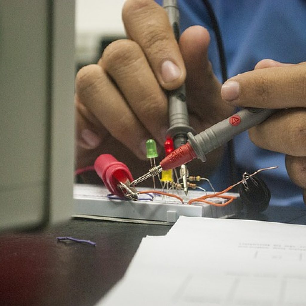
PCB assembly has many steps that benefit from visual inspection. Assemblers can select equipment for visual inspection based on the stage and target for the inspection. For instance, a visual inspection stage, with naked eyes, immediately after solder paste printing and device placement, can identify missing components, wrong placements, and contaminating solder paste. Our trained personnel can visually inspect solder joints after reflow by observing reflected light rays coming from different angles. In general, experienced inspectors can check about 5 joints every second.
Visual inspection validity, however, depends on the capability and consistency of the inspection staff, and the manner in which they apply the inspection standards. At Rush PCB, we train our inspectors to be aware of the technical requirements of each type of solder joint on a PCB. This is necessary as different assembly devices may have more than six types of solder joints, while each solder joint is capable of eight different types of standard defects. Therefore, it is impossible to apply visual inspection for quantitative measurements for effective structural process control.
Moreover, visual inspection makes use of regular light sources, and cannot help in inspecting hidden solder joints such as those under J-lead devices, BGAs, and surface array flip chips. Most of these devices are high-density packages. Based on uniform rules specifically established, the industry regards visual inspection as a technology with easy access, low cost, and applicable to inspecting large defects in small production runs.
Structural Process Test Inspection Systems
For large volumes of production, where accuracy and speed are of paramount importance, Rush PCB recommends structural process test inspection systems using digital equipment for automatic and real-time inspection and analysis, as these methods dramatically improve the capability and repeatability of visual inspection systems.
Most structural process test inspection systems depend on some form of light emission such as visible lights, lasers, and X-rays. They acquire data through real-time image processing for locating and measuring defects related to solder joint quality. Although these automated inspection systems do not need to physically contact the circuit board under test, they exhibit high repeatability and effectively eliminate subjectivity from inspecting and measuring defects.
Structural process test inspection systems may involve a variety of techniques depending on the complexity of the PCB assembly. These may include:
- Automated Optical Inspection (AOI)
- Automated Laser Test (ALT)
- X-ray Fluoroscopic System
- X-ray Lamination System
Selecting the method of inspection for the PCB assembly primarily depends on the defect type, inspection speed, and costs involved.
Automated Optical Inspection (AOI)
AOI systems typically use multiple visible light sources with programmable LEDs, video cameras, and computerized systems for inspecting solder joints. The graphics and intensity of reflected light from solder joints provides information on solder joint curvature. Analysis of this information helps to determine completeness of solder joints, sufficient quantity of solder, bad wetting, solder bridging, missing components, and displaced components.
However, use of visible light precludes inspection of hidden solder joints such as those under J-lead devices, BGAs, and surface array flip chips. AOI systems are suitable for inspecting solder joints at the rate of 30-50 joints per second, and for devices with pitch larger than 0.5 mm.
Automated Laser Test (ALT)
When it is necessary to measure the height and shape of solder paste deposition, Rush PCB recommends using ALT systems. The system measures the height and reflectivity of surface components by focusing a laser beam on them and measuring the reflection angles on multiple position sensitive detectors.
ALT systems provide data for real-time process control of solder paste printing including squeegee speed and stress, solder paste fluidity, cleanliness, alignment, and viscosity.
X-Ray Fluoroscopic System
By allowing a beam of rays from a single-point X-ray light source to pass vertically through the circuit board, the X-ray fluoroscopic system produce a density image to accurately inspect solder joint distribution, thickness, and internal integrity. By digitizing the image, it is possible to inspect for defects of solder joints such as cracks, inadequate solder, bridging, presence of voids, and misalignment.
X-Ray Lamination System
The X-ray lamination system uses X-rays to generate focal planes of a horizontal sectional area of a PCB. These are sectional images with surface thicknesses of 0.2-0.4 mm, allowing inspection of different sections of the same solder joint. This arrangement works perfectly for PTH and BGA solder joints.
Rush PCB recommends the use of the most appropriate inspection method for PCB assembly, depending on complexity, volume of production, and speed of inspection. As a rule of thumb, cost of inspection rises with the increase in complexity and speed of inspection.
Rush PCB guarantees quality of PCB assembly as we have highly skilled personnel and we use automated assembly machines. Call us or visit our website to get a free quotation for your assembly requirements today.


