

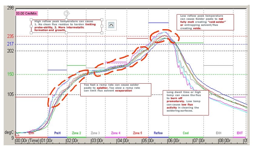
In Lead-free (Pb-free) reflow soldering for SMT PCBAs, soldering defects associated with thermal profiling can be mitigated by a thorough understanding of the variables affecting the process, as well as the metallurgical dynamics associated therewith. In Pb-free soldering, melt temperatures are typically higher, depending on the alloy used, and solderability is generally less robust than that of traditional Pb-based soldering. These factors can result in a narrower process window, never desirable. In this paper, we look at a brief outline of the reflow profile in general, with specific emphasis placed upon the hottest and coldest spots on the PCBA.
Pb-free Reflow Profile Guidelines
Preheat Issues
Effect:
Preheat Rate/Temperature Too High
Preheat Rate/Temperature Too Low
Cause:
- Thermo-mechanical stresses, e.g., the surface temperature of a component is higher than the interior temperature.
- Solder balling; solvents volatilize in flux; flux evaporation; oxidation of solder particles.
- Multi-axial stresses; affects board integrity, causing delamination in boards;
- Thermal shock; high preheat rate causes thermal shock to PWBs and components; component cracking;
- Cracks and damaged components; damage to heat-sensitive components, e.g., tantalum capacitors;
- Solder paste dry-out;
- Poor flux activation reduces solder joint quality affecting joint integrity;
- Cold solder joints;
- Poor wet-out of solder.
Soak Temperature Issues
Effect:
Too high a soak temperature
Too low a soak temp sotemperaturetemperature/time
Too long a soak (dwell)
Cause
- Solder paste dries out;
- Solder splattering and balling;
- Improper/ineffective flux activation;
- Solder paste dry-out;
- Excessive flux evaporation.
Time / Reflow
Effect:
Cause:
| TAL (Time Above Liquidus) too brief |
the joint may become trapped; |
decreases metal bonding action. |
|
| TAL too long |
|
|
|
| Reflow temperature too low |
formation. |
|
|
decreases metal bonding action. |
|
| Reflow temperature too high |
|
termination metallurgy dissolves into the solder. |
|
|
Reflow Effects on Solder Pastes
Pb-free profile guidelines: Locating the hottest and coldest spots on the PCBA
The temperature that solder joints reach, and the time above the melting point of the solder, are the result of a combination of three factors:
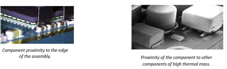
- Thermal mass of the component;
(Larger thermal mass = lower maximum temp. = less time above melting point)
- Proximity of the component to other components of high thermal mass;
(Nearer = lower maximum temp. = less time above melting point)
- Proximity to the edge of the assembly.
A Few “Rules of Thumb”:
- Nearer to PCB edge = higher maximum temp. = more time above melting point.
- Therefore, the coolest solder joints will usually be on large components, close to other large components towards the center of the assembly. The hottest solder joints will usually be on smaller components, in less densely populated regions of the assembly and closer to the edges of the assembly.
- Thermocouples should be attached to solder joints at the hottest and coldest parts of the assembly. This will help ensure that all joints reach a temperature higher than the melting point of the chosen solder and that no part of the assembly will become so hot that irreparable damage might occur. If the hottest and coldest parts of the assembly have not previously been identified, it is recommended that measurements be taken from at least six positions on the test assembly to identify them.

Why do we have both Hot and Cold spots?
| Component | Volume mm3 | Area mm2 | Volume/Area mm |
| CO603 | 1.02 | 40 | 0.026 |
| Board 141*208*1.6 | 46925 | 58656 | 0.8 |
| PLCC68 | 11250 | 5550 | 2.03 |
>> There is a huge difference in thermal mass in the BOM!
While maintaining a 235°C minimum solder joint temperature (= coldest spot), hottest spot might be well reaching the critical (potential) thermal damage limit.
Note: Although this is mostly the case, BGAs are NOT always the coldest spot!
Determining the hottest and coldest spots on a PCBA top side
- Apply solder paste on top side of printed board
- Mount all components on top side of the board
- Adjust oven to (*):
- Pre-heat zones: as normal settings (+/- 160°C) Reflow peak zones: as normal setting (+/- 280°C) Conveyor speed “full speed.
- Allow oven temperature to stabilize
- Pass board through oven
- Check: any paste dots molten?
- If no: decrease transport speed (e.g. with 0,05m/min) if yes, go to step 9
- Repeat steps 5, 6 and 7.
Procedure
- Apply some flux with a small brush to a board and pass it through an oven at reflow profile. Then pass the board up to 4 additional times through the oven.
- Take a new board with paste and components, when close to the hottest spot. Please clarify
- If some paste dots are molten: only a few dots (e.g., < 10).
- These dots are called Hot Spots (HS).
- If there are too many dots, go to the next step.
- If too many dots are molten: take a new board with paste and components,
- Increase speed in very small increments (0.01m/min), allowing oven to stabilize.
- Repeat steps 5, 6, 7 and 8.
- Now the Hot Spot(s) is/are known!
HOT SPOT: how to recognize it
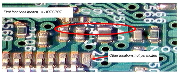
Other locations not yet molten
- Decreased speed of transport (with 0.05m/min).
- Pass the board through the oven.
- Are all paste dots molten? If no, repeat steps 14, 15 and 16 (WHAT steps???)
- If only a few (say < 10) dots are still not molten…
- Cold spot (to verify, repeat steps 14, 15 and 16)
- If ALL are molten, go to next step what one is that?
- If all dots are molten: take new board with paste and components. Take?
- Increase speed in very small increments (0.01m/min).
- Repeat from step 15 onwards (??)
- Now, the cold spot is known.

Determining the hottest and coldest spots on the bottom side
All other locations molten
Last remaining locations, not molten
= Cold Spot
Follow the same procedure as for the top side, But…
All components on top side also mounted!
REQUIRED MATERIALS (rule of thumb, but pending):
- Single Sided reflow board: For HS / CS determination on top side 1 to 3 boards.
- Double Sided reflow board: For HS / CS determination on top side and
Bottom side, 2 to 6 boards (2 for each side).
Determination of hottest spot and coldest spot requires up to 4 hours for one (1) board side!
Therefore, Double-Sided reflow SMT PC board requires up to 8 hours! But such efforts should be considered an investment in later smooth processing/control.
Rule of thumb: Follow profile advice of solder paste supplier, but also take into account the limitations of your components and PCB.
For High Temperature Organic Solderable Protective (HT-OSP) coatings it is recommended to use a nearly straight ramp profile in order to minimize the thermal load on the OSP coating during reflow soldering.


