


What Is a PCB Via and Why Manufacturers Fill Vias
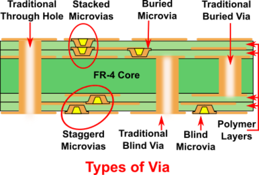
At Rush PCB, we manufacture various types of multilayered PCBs that require several layers to be electrically interconnected. A via is the most common way to make this connection. In general, a via is a plated through hole (PTH). The copper tube of the PTH terminates in copper pads at its end layers. If necessary, the copper tube may connect to other components, copper planes, or traces when passing through intermediate layers. However, if an electrical connection is not necessary in an intermediate layer, the copper tube passes through the layer unconnected. Since a via interconnects various layers, there are mainly four types of vias:
- Through-hole vias – Through-hole vias traverse the entire thickness of the PCB, starting from the topmost layer of the board and ending at its lowermost layer while interconnecting any internal layer, if necessary, by design.
- Blind vias – Blind vias start from either the topmost layer or the lowermost layer of the board and end at an intermediate layer while interconnecting any internal layer, if necessary, by design. Only one end of a blind via is visible on an external layer of the PCB.
- Buried vias – Buried vias start from an intermediate layer and end at another intermediate layer while interconnecting with any internal layer between the two, if necessary, by design. The ends of buried vias are not visible on the external layers of the PCB.
- Micro vias – Micro vias are created by using laser beams and are only one layer thick. In a multilayer board, several micro vias may be stacked one on top of the other or staggered to interconnect other layers.
We, at Rush PCB prefer that the barrel of all vias be filled or plugged, as this mitigates the challenges that unfilled vias can pose. Unfilled or unprotected vias can trap air, moisture, or cleaning fluids, can result in poor soldering, and cause structural weaknesses in PCBs. Briefly, manufacturers use two main fill categories:
Conductive filling – This method involves filling the via with a substance that conducts electricity, such as silver epoxy or copper paste. Conductive filling is ideal for applications that prioritize electrical and thermal conductivity.
Non-conductive filling – In this method, the manufacturer uses materials such as epoxy resin to fill the via. As epoxy resin is a non-conductor of electricity, this is a non-conductive filling and focuses on environmental and structural protection rather than on electrical performance.
Depending on the application, manufacturers may also planarize or copper-plate the end of a via, thereby creating a flat surface. This is especially necessary in via-in-pad designs.
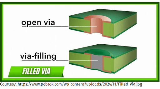
Process of Via Filling
The choice of via filling, whether conductive or non-conductive, depends on the application, the board’s cost and the production time.
Conductive Filling – Manufacturers use silver or copper epoxy to fill the holes. Being electrically and thermally conductive, these metals help in transferring electrical signals effectively while also improving the thermal conductivity of the via. Conductive filling helps to divert heat from large components like processors, microcontrollers, BGAs, and ICs.
Non-Conductive Filling – Manufacturers use non-conductive filling to improve the structural support to the pad such as in case of via-in-pad. They use epoxy paste or resin to fill the regular vias during the PCB manufacturing process. While the barrel of the via is filled with conductive paste, its wall is still plated with copper and conducts electricity.
Another option that manufacturers offer is plugging. While filling aims to occupy the entire via barrel, plugging may only partially close or cover the via opening.
Goals of Via Filling
Via filling has some common goals:
- Prevents contamination or corrosion – a filled via prevents entry of impurities
- Improves the mechanical strength of pads and vias
- Allows placing SMT components on the via holes
- Strengthens pad attachment, thereby enhancing board reliability
- Reduces solder wicking and solder related defects, leading to improved assembly quality
- Avoids trimming in silkscreen printing
- Conductive filling enhances the thermal conductivity and current carrying capacity of the via.
- Improving the life of the PCB, reducing the maintenance and replacement costs
When to Use Via Filling?
Deciding to use via filling depends on the specific requirements of the PCB. Some scenarios that benefit most from via filling:
Standard Consumer Electronics – Via filling provides the basic protection without adding unnecessary cost to PCBs for less demanding applications. Learn more about consumer electronics PCBs.
Harsh Environments – Environments such as those in aerospace, automotive, or industrial applications benefit from via filling as it protects against dust and moisture ingress and temperature extremes, thereby extending the lifespan of the board.
High-Power Applications – Designs involving significant heat generation due to high currents benefit from conductive via filling as the fill improves thermal dissipation and offers low resistance to high currents. This prevents overheating and potential failures.
High-Density Designs – HDI boards have tight spacing and use stacked vias. Conductive filling ensures reliable connections while supporting complex routing.
When to Use Conductive Via Filling
As conductive filling involves filling the via hole with a substance that conducts electricity, the filling becomes an active part of the circuit. Benefits of conductive via filling are:
Improved Thermal Conductivity – Conductive materials usually offer high thermal conductivity. In power-intensive designs, this helps dissipate heat efficiently, thereby preventing overheating while extending component life.
Enhanced Electrical Conductivity – Conductive materials like copper offer excellent electrical conductivity, making the assembly ideal for high-frequency applications.
Improved Signal Integrity – Conductive fills are good at reducing impedance mismatch which helps improve signal quality. This is often crucial for high-speed digital circuits that operate above 1 GHz.
Via-in-Pad Designs – With conductive filling creating a flat surface for via-in-pad structures, compact layouts benefit from reliable soldering and compact component placement.
Advanced PCB designs use conductive via filling to avail the above benefits, especially in industries like automotive, aerospace, and telecommunication.
When to Use Non-Conductive Via Filling
As a non-conductive via filling does not provide electrical conductivity, this type of filling is used mostly for applications that do not require additional electrical conductivity through the via. (Note that the via still provides electrical conductivity due to its barrel being made of copper, even though the filling is non-conductive). Benefits of non-conductive via filling are:
Blind and Buried Via Support – HDI designs mostly use non-conductive via fillings to stabilize the blind and buried vias. This ensures reliable layer stacking without having to add additional electrical paths.
Protection Against Contamination – Filling a via with epoxy seals it effectively from ingress of moisture, chemicals, and dust. In harsh environments like industrial areas, this is vital to improve the lifespan of boards.
Structural Reinforcement – Filling the via strengthens the PCB, thereby preventing deformations and cracking around the via. This is especially valid for multilayer boards with 6+ layers.
Cost-Effective Designs – As non-conductive materials are generally cheaper than conductive ones, a non-conductive via filling is more suitable for consumer electronic products, where high performance is not critical and budgets are tight.
Explain common goals: preventing solder wicking or contamination, supporting a pad, and improving thermal or electrical performance.
Non-conductive via fillings are especially helpful in applications that target cost savings and durability rather than thermal and electrical performance.
Conclusion
At Rush PCB, we choose conductive fill when conduction through the fill is required. We select non-conductive fill when the PCB requires support, sealing, and soldering reliability.
FAQ
What is difference between conductive and non-conductive via filling?
As the name suggests, conductive via filling is metal based. It allows current flow and is thermally conductive. Non-conductive via filling is epoxy based. It does not allow current flow and is thermally non-conductive.
When is conductive via filling preferred?
When the design requires maximum thermal and electrical conductivity, mainly for high-power applications. HDI designs that use small-diameter vias also require conductive via filling.
When is non-conductive via filling necessary?
Applications that do not require thermal and electrical conductivity use non-conductive via filling.
Why is it necessary to fill vias?
Manufacturers fill vias with conductive or non-conductive material mainly to eliminate the void that can trap air, moisture, chemicals, or contaminants, thereby preventing assembly-related failures.
Why do you need micro vias for HDI PCB design?
As HDI PCBs use highly compact layouts, there is no space available for regular vias. Micro vias are created using laser beams and they are far smaller in diameter as compared to regular vias. Using micro vias improves routing efficiency in HDI PCBs. They shorten the electrical paths or traces and help in supporting fine-pitch BGAs.
Are filled vias beneficial?
Yes. While non-conductive via fills provide mechanical and structural support to the board, conductive via fills improve electrical and thermal conductivity.


