

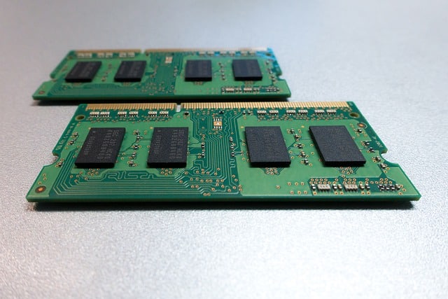
All electronic equipment require a printed circuit board or PCB to function to their intended performance. Eminent PCB manufacturers such as Rush PCB Inc fabricate boards for their customers in the most effective way, so that they can produce the boards most economically. One of the methods they use is PCB panelization, which involves grouping the boards such that from a standard panel they can produce the maximum number of boards with the least wastage. After the assembly and testing is complete, a breakout process produces individually working boards.
PCB Panelization
Manufacturers use PCB panelization as a method where they can group and process small circuit boards as an array within a standard copper clad panel. Not only does this method manage to fabricate boards economically, but also facilitates their easy movement through the assembly process. Most machines in the assembly shop have conveyors with standard widths.
With panelization, PCB manufacturers can make smaller boards fit into the standard conveyors in the manufacturing process, thereby making manufacturing the boards more effective. PCB panelization offers several benefits:
- Improved Production Throughput — For manufacturing involving a large number of boards, panelization helps to minimize costs while reducing lead times.
- Safe & Efficient Handling — Handling a large panel made of many small boards is safer and more efficient than handling them individually.
- Improved Process Speed — Panelization improves overall processing speed. This includes better timings for paste printing, component placement, soldering, and quality inspections.
- Reduces Scrap and Wastage — With panelization, it is possible to make the maximum use of standard copper clad panels. Reduction in scrap and wastage leads to lower costs.
PCB Panelization – Factors to Consider
Although there are multiple factors that affect PCB panelization design, three are most important:
Circuit Board Design
The most suitable panelization technique depends to a large extent on the design of the circuit board. Here, the clearance between the components and the PCB edge is an important factor.
Components on the Board
Components are an integral part of any circuit board. They provide the board with its unique features that make it suitable for its intended functions. However, their placement on the board affects the panelization design applicable. It is preferable to locate delicate and sensitive components as far away as possible from the edges of the board, as the activity of depanelization may cause them damage.
PCB Material
The material of the circuit board has a strong influence on the panelization method, as some materials are more prone to splintering during a breakout. The thickness of the board is another major factor. While thin boards are susceptible to splintering during the breakout process, thicker boards are more difficult to break.
PCB Panelization – Design Guidelines
PCB panelization design must be a part of the primary circuit board design and the designer should not include it only as an afterthought. Once the designer has decided on the layout of a single board, they must use the computer-based design system to replicate the layout in an array that best fits the standard copper clad board their manufacturer has recommended.
This requires the designer to contact their manufacturer to know the size of the standard copper clad boards the manufacturer uses. The designer will also need to know the tooling hole locations in the rails necessary to incorporate them in their design.
PCB Panelization – Techniques
In the panelized board, individual PCBs will connect to one another in an array form. There may be extra board material in the form of rails to make them fit the conveyor belts of automated machines. The rails usually have tooling holes for guiding the panel in the machine. As ultimately, operators must separate or depanel individual PCBs from the panel, the designer must provide them with the means for breaking out the sections.
Three methods of depanelization design are in popular use:
V-Scoring
The manufacturer makes a v-shaped grove for distinguishing individual circuit boards in a panel. Typically, the grooves are present on both sides of the board, to a depth of about one-third the PCB thickness. Operators mostly use a tool to break out the individual boards.
Solid Tabs
Manufacturers use the presence of small solid tabs between individual circuit boards. They provide the panel its required stiffness. For depaneling or separating individual boards, operators use laser cutting equipment or a depaneling router.
As solid tabs require more effort in depaneling, and the process generates a lot of dust and vibrations, most manufacturers do not favor using solid tabs.
Tab Routing
As an alternative to the above methods, manufacturers prefer to use tab routing. Here, they separate each board with tabs, with each tab having 3-5 holes in a line. Operators use edge-hanging tools for depanelizing, with the tabs breaking away along the holes. This is a more convenient panelization method, as the operators can use both manual or mechanized breaking methods for depaneling the boards.
Conclusion
PCB depanelization is a process requirement that benefits both the manufacturer and the customer. Most reputable and professional PCB service providers, such as Rush PCB Inc, recommend using PCB panelization techniques, as they offer substantial cost benefits along with minimizing waste.


