PCB Fabrication Processes
Image Source: http://www.zowyeh.com/PCBA/PCB%20Fabrication/process.html
PCBs have been developing since the 1950s. During the last sixty years, there have been ongoing changes in technology, and in the manufacturing of PCBs. Key changes in the fabrication of PCBs have included the development of double-sided boards, the ongoing miniaturization of the components, the establishment of standards for PCBs, and the use of surface mount technology.
PCB Fabrication Steps
Designers will want to maximize the potential of your PCB by maximizing the use of space and performance of your board. It may be worth consulting with a circuit board expert to ensure that your PCB design and resulting order are processed without unnecessary delays.
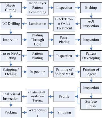
There are many steps involved in fabrication of PCBs. Once you’ve finalized your design, the PCBs are grouped onto a larger board (a panel) for bulk printing. The panel may include a single design of PBC, or multiple designs. Once the panel is prepared, the pattern of the board is replicated using a CAM system with copper foil PCB layers. Etching then removes unwanted copper. In this stage, silk screening, photoengraving or PCB milling is used to etch the board. The method of etching used will vary based on the number of boards to be produced, and the required resolution of the boards. The copper can be laid using subtractive, additive and semi-additive processes.
In a subtractive process, a complete film of copper is laid, and then the unwanted parts are stripped to leave the desired pattern. In an additive process, the required copper is electroplated onto the substrate. Additive processes use less material and generate less waste. Semi-additive processes are the most common. In this process, the board has an initial thin layer of copper. A reverse mask is then applied, which exposes the parts of the substrate that become traces. Other surface platings are then applied.
Following automated optical inspection, a lamination process is used to generate separated layers. The PCB is then drilled with small diameter tungsten-carbide drill bits, specially designed to ensure they don’t tear the traces. As an alternative, drilling may be completed using a laser to provide a very small vias. The holes may be conductive (by electroplating or using eyelets). Holes can be depth-controlled to allow conductivity to specific layers only.
The PCBs are then plated with solder to provide a resistant surface for etching. Areas that aren’t going to be soldered are covered with solder mask. The legend is silk-screened or photo imaged. Before components are added, the boards are tested to ensure appropriate connectivity. Once the board is validated, the components are assembled for form a functional PCA (Printed Circuit Assembly).
The final stage of fabrication is applying a coat to prevent corrosion and leakage.
The fabrication process is undergoing change, as manufacturers seek to deliver their products in a manner that minimizes the potential risk for their production workers from the various chemicals used in the processes such as lead. Lead has been used in the fabrication of PCBs, but greater awareness of the health impacts has resulted in a change in fabrication technologies. Printed Circuit Design and FAB have highlighted health issues in a recent publication, noting that the drive for change in chemical processing is being driven by NGOs.


