

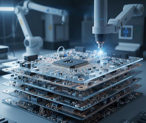
As electronics become smaller, faster, and more powerful, Printed Circuit Board (PCB) technology must advance in parallel. Modern ultra-thin high layer count rigid PCBs used in computing, telecom, medical, and aerospace systems can pack 20 to 30 layers into less than 1.2 mm thickness. Achieving this performance demands high precision, as handling thin materials, fine copper traces, and multiple laminations is extremely challenging.
At RUSH PCB Inc, we explore the key manufacturing and assembly challenges of ultra-thin, high layer count PCBs and the advanced methods that are used to overcome them.
Material and Core Thickness Constraints
The first challenge arises from material selection and core thickness management. To achieve ultra-thin constructions, fabricators use dielectric cores as thin as 25–50 µm and copper foils of 1/3 oz or less.
However, these materials come with several challenges. Ultra-thin cores are mechanically fragile and can be damaged easily during handling or imaging. They also tend to expand or shrink with changes in temperature or humidity, leading to dimensional instability. In addition, even small variations in dielectric thickness can affect controlled impedance, which is critical for maintaining consistent signal transmission in high-speed circuit designs.
To improve reliability, manufacturers often use low-flow prepregs (specialized adhesive sheets that control resin flow during lamination) and reinforced epoxy systems for better rigidity and thermal performance. Despite these advances, thin material handling remains a critical source of yield loss.
Layer Registration and Alignment
As the number of PCB layers increases, maintaining accurate layer to layer registration (precise alignment of internal copper layers) becomes increasingly difficult. Even a slight misalignment of just 25 microns (1 mil) can lead to shorts or open circuits in high density designs. Several factors contribute to this challenge, like:
- Thin cores can deform under lamination heat and pressure.
- Uneven copper distribution can cause differential expansion and pattern distortion
- Reduced overall rigidity in multi-layer stacks can make traditional pin-based alignment methods less reliable.
Advanced fabricators address these issues with optical and X-ray alignment systems, pin-less lamination, and automated lay-up systems that maintain tight registration accuracy. Still, controlling registration in 30+ layer PCBs remains among the most complex manufacturing challenges.
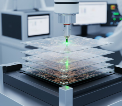
Lamination Process Control
The lamination process which bonds multiple inner layers into one composite, is the heart of multilayer PCB fabrication. However, it presents several critical challenges, like:
- Resin Flow Control: Controlling resin flow is essential, as excessive flow can result in resin starvation or voids within the dielectric.
- Pressure Uniformity: Maintaining uniform pressure during lamination is equally important, since uneven pressure can lead to delamination or board warpage.
- Sequential Lamination: In high layer count PCBs, sequential lamination cycles are often required, which can introduce dimensional shifts and increase internal stress within the board structure.
Manufacturers use multi-zone vacuum lamination presses (equipment that controls temperature and pressure across zones) to ensure consistent curing. Controlled heating and cooling profiles are also used to prevent internal stress buildup. Even minor variations can drastically impact yield in ultra-thin stacks.
Drilling and Via Formation
After lamination, via formation becomes one of the most critical and challenging steps in multilayer PCB manufacturing. Vias (the tiny holes that electrically connect different layers) must be drilled and plated with extreme precision. Several issues can occur during this process like:
- Thin boards tend to lack mechanical rigidity, increasing the risk of drill wander and hole misalignment.
- Resin debris left behind after drilling can cause smear formation, preventing proper copper contact.
- High aspect ratio vias, which are deep and narrow, are particularly difficult to plate uniformly.
Laser drilling is commonly used for creating microvias with diameters below 100 micrometers, as it offers high precision and causes minimal mechanical stress on the PCB. After drilling, a plasma de-smear process is applied to remove any resin residue and ensure clean copper surfaces for reliable plating. Despite these advanced techniques, maintaining consistent via quality through multiple lamination cycles remains a highly specialized and tightly controlled manufacturing process.
Bow and Twist Control
Board warpage (bow and twist) is a common issue in ultra-thin, high layer count rigid PCBs. These distortions usually occur because copper and dielectric materials expand at different rates when exposed to heat, or due to uneven copper distribution across the internal layers. Such deformations can cause several problems during manufacturing and assembly, like:
- All of the component pins may not make electrical contact with the land pad, leading to placement errors.
- Warpage can also result in poor solder joint formation, affecting electrical reliability.
- Additionally, it creates challenges during Automated Optical Inspection (AOI) and Pick & Place operations, making the overall assembly process more difficult and less accurate.
To minimize bow and twist, several mitigation techniques are used. One effective approach is to keep PCB stack-up construction symmetrical, which helps balance mechanical stress across the PCB. Even copper distribution across all layers also plays a key role in preventing uneven expansion and contraction.
Assembly Challenges
Once fabrication is complete, PCB assembly introduces another set of complications. The thinness and complexity of these boards demand precise thermal and mechanical control during component soldering.
1. Handling and Support
Ultra-thin boards are prone to flexure (bending due to weight), which can lead to:
- Component misalignment during placement
- Cracked solder joints during reflow.
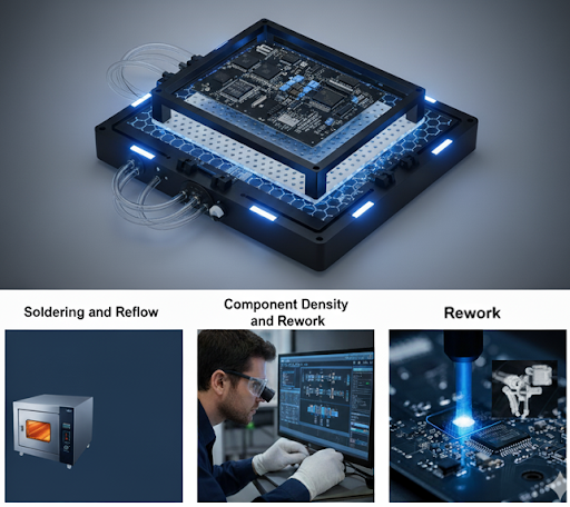
To counter this, assemblers use vacuum fixtures, carrier frames, or stiffeners during Surface Mount Technology (SMT) processing to maintain board flatness.
2. Soldering and Reflow
Ultra-thin high layer count rigid pcbs tend to heat up quickly and unevenly in reflow ovens. This uneven heating can lead to common soldering issues such as solder bridging, tombstoning, or even delamination of the PCB layers.
To prevent these problems, it is important to carefully optimize the reflow temperature profile, control preheat ramp rates, and, when necessary, use nitrogen atmosphere soldering. These measures help maintain strong, reliable solder joints while ensuring that the board’s temperature stays below the glass transition temperature (Tg) of the dielectric materials.
3. Component Density and Rework
High-layer-count designs often feature fine-pitch BGAs (Ball Grid Arrays), CSPs (Chip Scale Packages), and 01005 passives. Because these components are placed so close to each other, it becomes difficult to reach and repair individual parts without disturbing adjacent ones. If too much heat is applied during rework, it can easily damage the ultra-thin dielectric layers inside the PCB, leading to delamination or reliability issues.
Modern assemblers use localized reflow systems, low-melting solder alloys, and X-ray-guided rework stations to safely repair defective joints without warping the board.
Making Complex PCBs Efficient and Reliable!
At RUSH PCB Inc., we understand that precision manufacturing for ultra-thin, high layer count rigid PCBs comes with added complexity and cost. These advanced boards often require multiple lamination cycles, specialized materials, precision drilling, and extensive inspection, each step increasing production challenges and affecting yield. Once layer counts exceed 30, yields can drop significantly, driving up overall cost.
That’s why we work closely with our customers to explore smarter alternatives such as rigid-flex or HDI sequential buildup designs, which deliver the same high electrical performance with improved manufacturability and cost efficiency. Our goal is to ensure your complex PCB designs are not only possible but produced efficiently, reliably, and at the best value.


