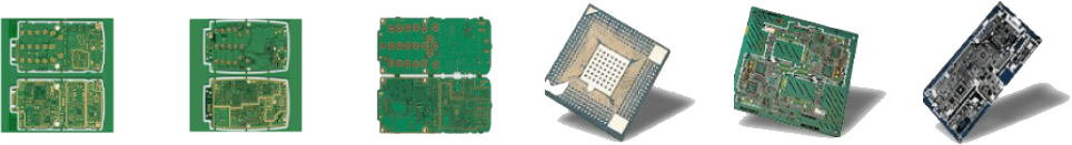
Hdi Capability
Template: desktop two
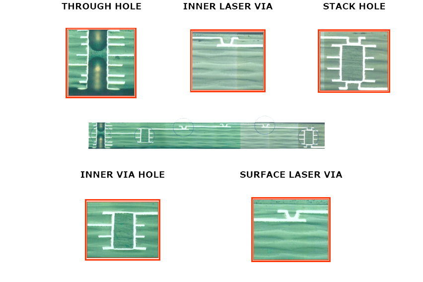
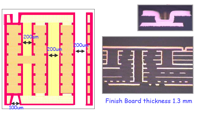
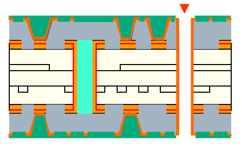
HDI Technology in Hole
High Density Interconnection
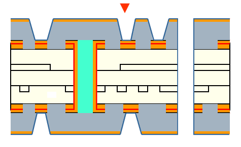
Blind & Burried 9+2+9 Laser Drill
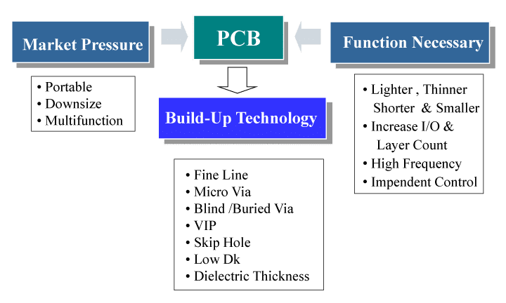
Market Trend vs. Technology Solution
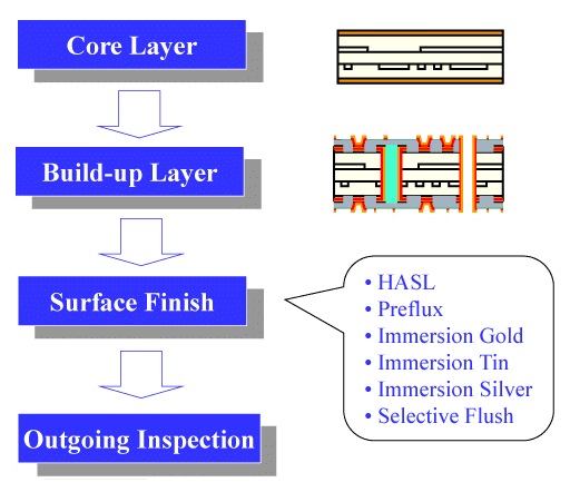
HDI Process Flow
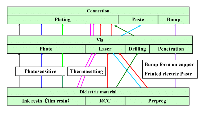
Main Process of Build – up Layer
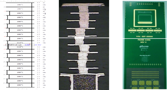
Construction Materials
Material Type
- FR 4 Tetra Function ( Tg. 130 – 140 ℃ )
- FR 4 High Tg ( Tg. 160 – 180 ℃ )
- RCC ( Tg. 150 ℃ & Tg. 185 ℃ )
- Ink ( VIL )
Comparison of Material
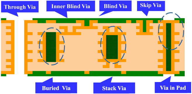
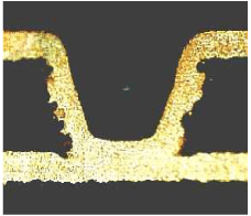
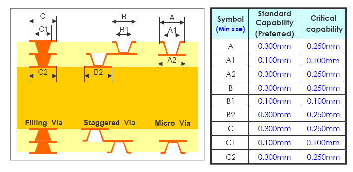
Comparison of Via Technologies
Comparison of Blind Via
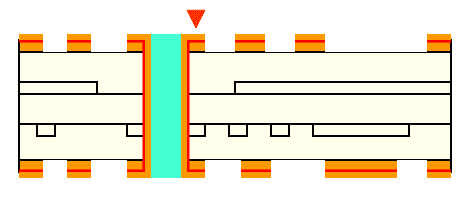
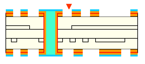
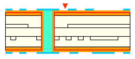
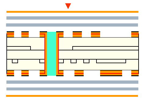
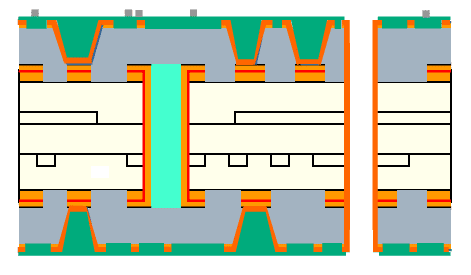
Build-up for 2 + N + 2
1+6+1 without buried, extend to 1+N+1
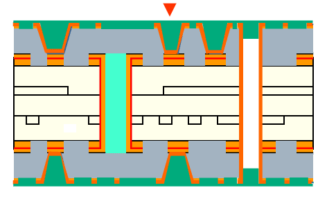
1+4+4+1 with buried via, extend to 1+N+N+1
Black Oxide Treatment
D.F. Exposure / Developing
Dry Film Lamination
I.V.H.Grinding ( for thickness >= 60 mil )
Inner Via Hole Plugging ( for thickness >= 60 mil )
Electroless Copper Plating
I.V.H.(Inner Via Hole) Drilling
I.V.H.(Inner Via Hole) Drilling
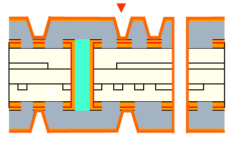
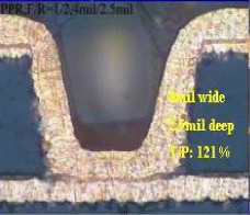
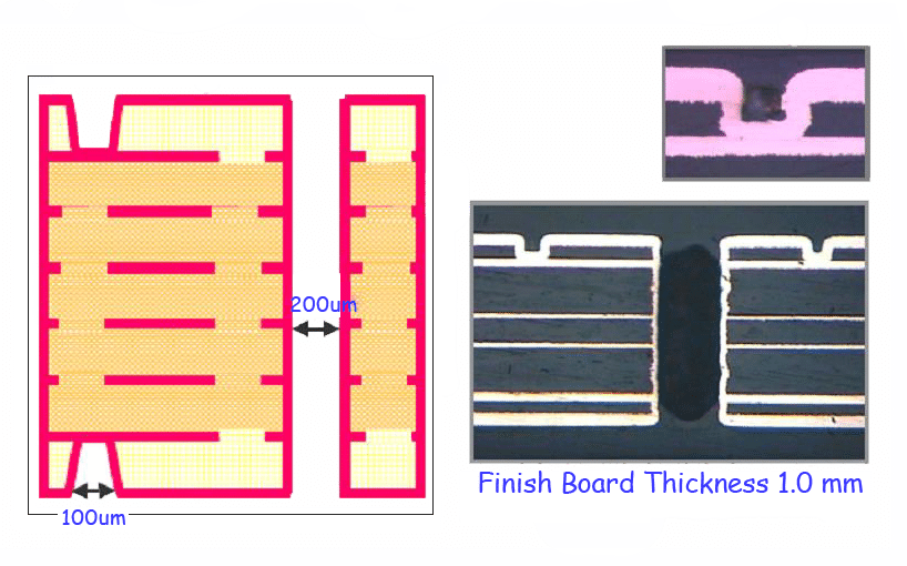
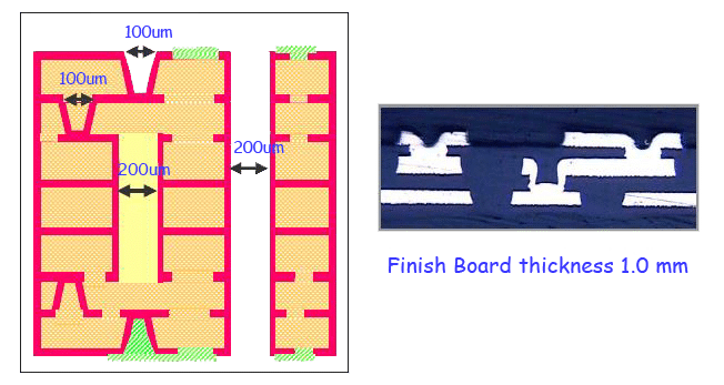
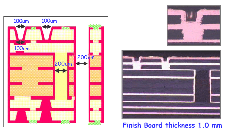
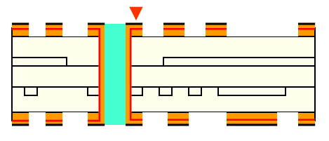
Blind via Capability
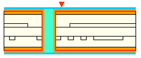
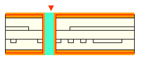
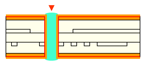
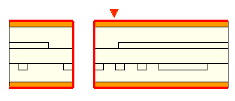
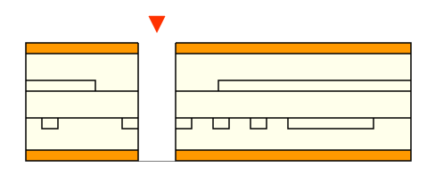
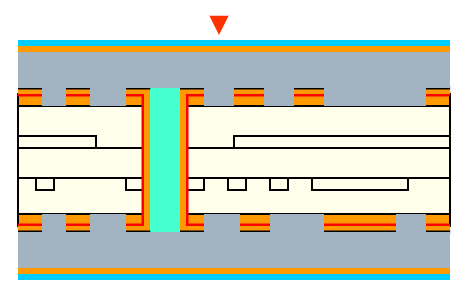
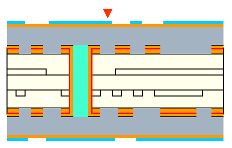
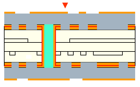
2+4+2 Staggered via, extend to 2+N+2

2+4+2 Staggered via, extend to 2+N+2
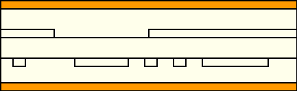
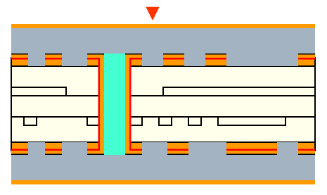
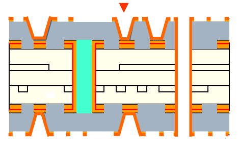
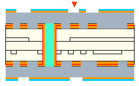
2+4+2 laser via on laser via
Solder Mask Printing
Dry Film Lamination
Lamination
Prepreg Layup
Black Oxide Treatment
D.F. Exposure / Developing
D.F. Exposure / Developing
Electro Plating
Desmear / Electroless Copper Plating
D.F. Strip
Etching
S/M Exposure / Developing
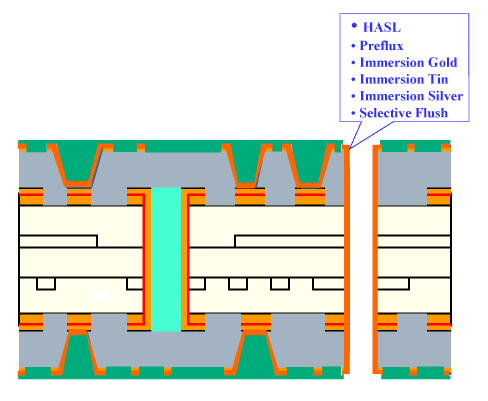
Surface Finish