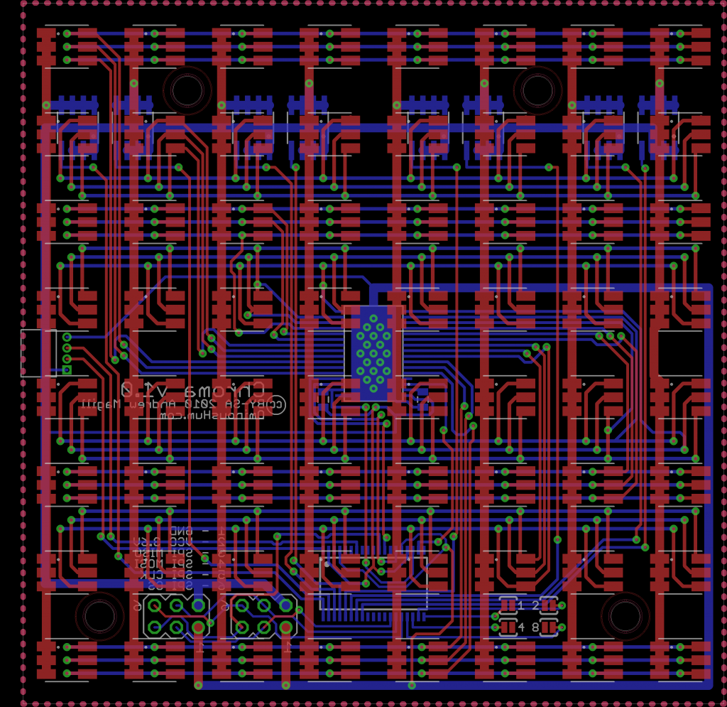
There are many steps to finalizing the design of a PCB. Engineers who are aware of the risks in design and can plan for them will have a more productive output. These are some of the common ways of avoiding errors in designing PCBs.
Plan!
Make sure that you’re using the right tools. While there are many EDA packages available, you will need to be aware of the strengths and limitations of the software. For example, some packages have issues such as footprint mismatches. Ensuring the design is correct at the planning stage will avoid challenging issues in later development. EDA packages may include component footprint libraries. It will be worthwhile checking that the detail in the libraries is correct for each component.
Engage with other team members
A team that works together, understanding the desired outcome will help ensure an effective PCB design. Each team member will have a different perspective, and may be able to identify possible design issues, early in the process. In any field of endeavor, most people will miss errors in their own work. That’s why it is important to have someone else review and critique the design. Experience can be as valuable as theory. An experienced technician can help identify issues. Designers and engineers need to have an ongoing and effective communication process in place.
Making sure the prototype meets specifications
Ensuring that the prototype meets all functional requirements will help minimize the risk of mistakes being present when the PCB is in production. Make sure you have comprehensive prototype testing protocols in place. Develop a test plan, and identify objectives of the testing process. It is a better process to identify issues, create new prototypes, and re-test than it is to short-cut the prototype stage and risk downstream errors. Include testing of high-risk elements.
Substitutions
Board layouts need to be correct for the proposed design, and meet the potential requirements of substitute components. If a substitute component has a slight variation in characteristics, is may be sufficient to affect the performance of the whole design. Some components will be more tolerant of substitution parts, while others will need to operate within a highly specific range. An error that occurs from a substituted component oscillating and behaving erratically can be challenging when you’re in the troubleshooting stage. Check the datasheets for components to help minimize the risks.
Having detailed documentation and silk-screening
Once the PCB is made, silk-screens will be the main way others will interact with the PCB design. They need to be as thorough as possible. For example, issues can arise when detail such as polarity isn’t clearly identified. Components such as diodes, electrolytic or tantalum capacitors should be clearly marked. Similarly, the first pin should be clearly marked wherever possible, and orientation should be marked for IC packages and components.
Backing Up
While it is an obvious thing to do, it is amazing how often hours of work are wasted through a failure to back up.


