

Why Ground Planes Are Better Reference Planes than Power Planes in PCB Design?
In high speed PCB design, keeping signals clean and stable is essential to ensure the system runs reliably and performs as expected. One of the most important factors that affects signal integrity is what lies beneath the signal trace, the reference plane you choose. Designers commonly use either ground (GND) or power (VCC) planes as reference layers for routing signal traces. At first glance, both might appear equally suitable since they are conductive but their behavior in high speed circuits is quite different.
In this article, we at RUSH PCB Inc will explore what happens when a power plane is used instead of a ground plane as the reference. By breaking it down with simple, everyday examples and clear illustrations, we’ll try to make the concept easier to understand.
The Concept of a Reference Plane
When a signal travels along a trace on a PCB, it always has a companion “the return current” which flows through the nearest conductive layer beneath it. This underlying layer, known as the reference plane, provides a path for the electromagnetic energy that surrounds the signal trace.
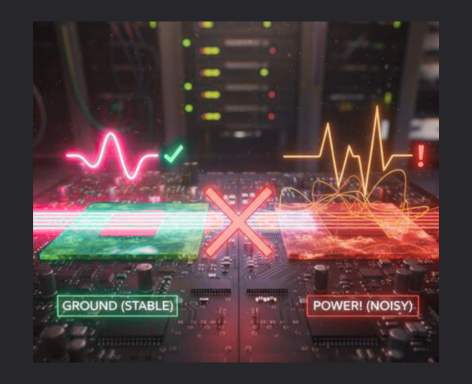
If the signal layer references a solid ground plane, the return current naturally flows right under the trace, creating a tight, low inductance loop. This arrangement helps reduce electromagnetic interference (EMI) and keeps the characteristic impedance stable, which is ideal for high-speed performance.
But things change when the signal references a power plane instead. In this case, the return current cannot flow directly beneath the trace, it must find its way back to ground through decoupling capacitors that connect the power and ground planes. This longer, indirect path increases the current loop area and can disrupt signal integrity, leading to unwanted noise or reflections in the system.
Try to understand the concept with the following example:
Imagine driving on a highway that has a smooth road running directly underneath it providing a way back home, that’s like a ground plane.
But, if the return road is far away (reference is a Power instead of a GND plane), and you have to take a long detour through a roundabout (the decoupling capacitor), the trip becomes longer and more confusing. In PCB circuit, this is similar; the longer return path creates more noise and interference in the signal.
Case Comparison: Ground Plane vs. Power Plane Reference
Case 1: GND Plane as Reference (Ideal Condition)
When a signal trace runs over a solid ground plane, the return current flows directly beneath it, forming a compact loop. This tight coupling between the signal and its return path ensures smoother, more reliable transmission.
Having GND as reference plane gives following benefits:
• Clean and stable signal flow
• Minimal electromagnetic interference (EMI)
• Consistent impedance control
• Reduced sensitivity and strong immunity against the external noise
Case 2: Power Plane as Reference (Problematic Condition)
If the same signal runs over a power plane, the return current must find a decoupling capacitor to cross from power to ground. If the capacitor is not close to the signal path, the return current must travel a longer route, forming a large loop.

Using a power layer as the reference plane can lead to the following issues:
- Increased EMI due to the larger loop area
- Signal integrity degradation
- Noise coupling from power fluctuations
- Possible reflections and impedance mismatches
Understanding Reflections (Ringing and Overshoot)
When high-speed signals switch rapidly between logic states, even a small discontinuity in the return path or impedance can cause unwanted signal reflections. These reflections often appear as ringing or overshoot in the signal waveform.
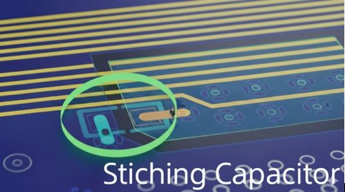
If a decoupling capacitor is placed too far from the point where the return current transitions between planes, the longer path introduces inductance. Because inductance resists quick changes in current, this delay causes a brief voltage spike known as overshoot. The excess energy then bounces back and forth along the trace, creating the oscillations we observe as ringing in the signal.
Why a Ground Plane is the Best Reference for Signal Integrity?
A ground plane keeps the PCB stable and noise-free. It maintains a steady voltage level, provides a short low-impedance return path, reduces EMI by keeping the loop area small, and ensures predictable impedance for reliable signal performance.
Best PCB Design Practices
To keep signals clean and stable, it is best to route high speed traces over a ground plane. When a signal switches layers, place decoupling capacitors close to the vias so the return path stays short and smooth. Keep power and ground planes close together by using thin insulation layers (4 mil or less) to cut down noise. Also, add proper terminations like series or parallel resistors to prevent reflections and ensure reliable high-speed performance.
Read More: What is AOI and its Importance in PCB Assembly
Our Expertise
At RUSH PCB Inc., our EE expertise ensures every design performs flawlessly at high speeds. At times engineers have no choice but to use power planes as the reference plane which may seem fine for low frequencies but often causes noise and instability at higher ones. That is where our expert engineers embed the solutions in the proper stack-up design with meaningful arrangement of power and ground planes to ensure clean, low impedance return paths and superior signal integrity of higher speed interfaces. We share instructions as well as monitor the placement of the high frequency bypass caps in the region. We ensure a reliable product free of ringing, overshoot, reflections and EMI out of smart stack-up design and careful placement of high frequency decoupling caps.


