The advent of revolutionary new products, driven by miniaturization of components and semiconductor packages supporting advanced features, is driving the Printed Circuit Board (PCB) industry to increase the functionality of their boards within the same or reduced areas. This includes products such as the hand-held touch-screen computers, 4G network communications, and industrial and military applications such as smart ammunitions and avionics. Eminent PCB manufacturers such as Rush PCB Inc. are providing solutions for the above with High Density Interconnect (HDI) boards.
HDI PCBs use high performance thin materials as prepregs, have fine copper lines, and use the Every Layer Interconnect (ELIC) technology to offer very thin flexible PCBs with very high functional density per unit area. Advanced HDI PCBs make use of multiple layers of copper filled stacked in-pad micro-vias that enable interconnections with even greater complexity.
Rush PCB Inc. is currently building a 10-layer board with an FR4 grade prepreg (TUC-872SLKSP), starting with all layers of 1/3 oz. copper. The outermost layers of copper will be coated with Electroless Nickel Immersion Gold (ENIG), and covered with a coverlay (green mask) of thickness 0.0249” ± 0.003”. Component placement will be aided by a printed white silk screen, while the width and spacing of copper traces in each layer has been carefully calculated to give precise control on the impedance. The board has an overall size of 6.857” x 5.287” and its model number is 104-032-01 Rev 10. Rush PCB Inc. will be manufacturing 100 Numbers of this HDI PCB with a lead-time of 9 days.
Stack-Up Design
Before finalizing the design of multi-layer PCB circuit boards, designers need to confirm the structure of the circuit board primarily based on the scale, physical size, and the requirements of electromagnetic compatibility (EMC). Considering the above, designers at Rush PCB Inc. have decided to use 10 layers of circuit boards. This also decided the placement of the inner layer and the manner of distribution of different signals in these layers—the stack-up design of the multi-layer PCB. This careful planning and rational selection of the stack-up design beforehand will be saving the user a huge effort in wiring and production later.
Two major factors need to be decided once the designers have determined the number of circuit board layers. These are the distribution of the special signal layers and the distribution of the power and ground layers. However, with multi-layer circuit boards such as the 104-032-01 Rev 10, designers at Rush PCB Inc. followed some general principles to obtain the best combination of signal, ground, and power layers:
- The signal layer was kept next to an internal power or ground layer, shielded by the copper film of the internal power layer.
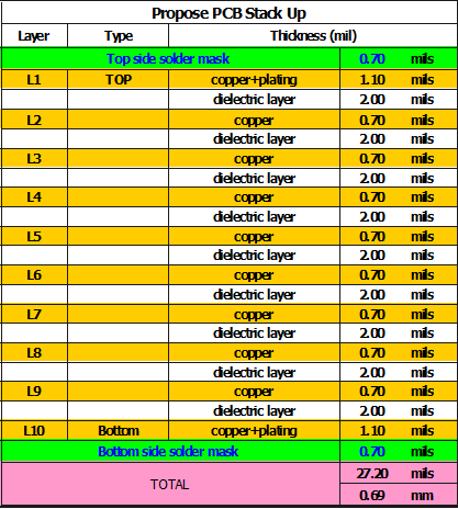
- To keep a tight control over the impedance, the internal power layer was integrated tightly with the ground layer, so that the thickness of the prepreg between the internal power and ground layers was kept thin, of the order of 2.00 Mils.
- To minimize crosstalk, no two signal layers were kept adjacent each other. As far as possible, the designers placed a ground layer in between two signal layers to avoid crosstalk.
- To control the ground impedance, designers placed multiple grounded internal power layers.
- The layer structure was designed to be symmetrical.
The final stack-up is shown in Fig.1. The overall PCB thickness is only 27.20 Mils or 0.69 mm.

Every Layer Interconnect Technology
To achieve very high-density interconnection, designers at Rush PCB Inc. have used the Every Layer Interconnect (ELIC) technology. This is a method where each layer has its own copper filled laser-drilled micro-vias. When stacked up, it provides the opportunity for dynamic connections between any two layers in the PCB. Not only does this offer an increased level of flexibility but also maximizes the circuit density. The designers took up the additional complex challenges in routing with Via-In-Pad (VIP) and employing blind and buried vias. Laser drills were used for drilling the via holes, and they were filled up with conductive copper paste.
PCB 104-032-01 Rev 10 uses a total of 32 sets of blind and buried vias between the following layers, as shown in Fig.2:

Impedance Control
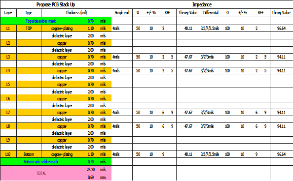
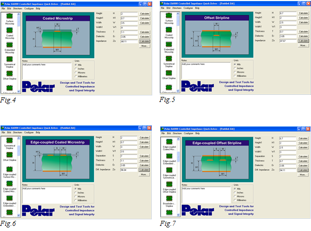
Designers at Rush PCB Inc. have referenced the signals on the top and bottom layer to the ground plane next to them. Likewise, signals on other layers are referenced to ground planes adjacent to them. High-speed signal routing on an inner layer is sandwiched between ground and power planes. Careful design of trace width, spacing, and prepreg thickness has led to a tight control over single-ended and differential impedance as shown by calculations in Fig.3, Fig.4, Fig.5, Fig.6, and Fig.7:
Read About: BGA ROUTING AND IMPEDANCE CONTROL IN HDI PCBS
Fig.3


