

In today’s world, the demand for cutting edge high speed electronic devices has not only complicated the design and layout process but has also impacted the manufacturing industry as well. PCB layout is the blue print of the design. We can plan to design anything in the schematics and using CAD tools on PC, we can layout anything in any way but once it is laid out, can it be manufactured?
If it can be manufactured, will it function as per desired parameters?
If it is working in the lab, is it guaranteed that it will function properly in the outer world in presence of all other electronic products, meeting all the radiation regulations??
The cost of the final product is yet another factor that we have to monitor and keep in mind.
These are a glimpse of some of the key questions that we have to answer before we decide to invest in any design. We don’t have the luxury of laying out anything as per the requirement of design and assume that it can be manufactured.
If someone asks me, one of the most important sections of the electronic product design that impacts the mechanical, thermal, electrical, functional and financial aspects of this journey, I would probably name it the PCB STACK-UP DESIGN which impacts all of these. PCB stack-up is one of the key aspects of the electronic product design that plays an important part in keeping all the parameters under check and control. At Rush PCB Inc., our engineering team is well aware of these skills and knowledge that is required for initial design work for large, dense PCBs, especially the High-Density Interconnect (HDI) types, to define the appropriate stack up and enable the creation of an effective board. Stackup design acts like a backbone in the overall design structure of a PCB which when described in simple words is nothing more than an arrangement of conductive and insulating materials but its impacts are very vast and far reaching. We work closely with our customers during the design of the HDI layer stack-up, as this helps to minimize the cost and to meet requirements of signal integrity. When we both agree to an HDI layer stack-up prior to designing the board, the fabricator will need to make only minimal adjustments to comply with your requirements.
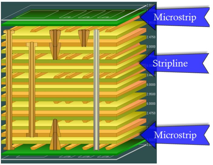
The below picture shows some of the modern day aspects of an electronic design that are strongly associated with the stackup design.
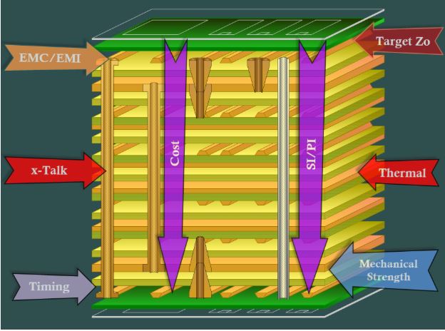
Let us briefly study how they are stitched into the stack-up design.
Stack-up Design – Cost of the PCB:
Cost is one important and major factor that we must consider while designing the stack-up. Costs vary based on materials used and the number of layers in your stack-up. At Rush PCB Inc., we work with our customers to make sure we are using materials that are both cost efficient and yet meet their design requirements. Whether or not to add a power plane, number of ground planes, etc. can be beneficial to the design and impacts the cost – but it all comes down to how we approach and understand the design requirements. Higher number of layers means more material which means higher cost. There might be many factors impacting and dictating the number of layers in a PCB. Few important ones are as follows:
1- The total number of nets in the design. A higher number of nets would need more layers to complete the routing.
2- Complexity of connectivity and hot-spots due to crisscrosses in connectivity would generally require more layers to resolve conflicts and achieve complete routing.
3- The presence of parts like high pin density BGAs that have larger pin counts with smaller pin pitches and greater pin-depths would always demand extra routing layers to fan-out such parts and close the connections of nets and buses coming from these parts.
4- The density of the placement of the components in the design also impacts the stack-up demand for more layers.
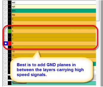
5- SI concerns related to sensitive and high frequency nets require separation between nets both in xy and z—direction as well. They need GND planes in between the signal layers. Sometimes having GND planes above, below and to the left and right of the signal layers is mandatory to meet the target impedances and the noise margins. This all translates into more layers in the PCB stack-up.
6- Sometimes due to high-current applications, single power plane copper is not sufficient to carry the huge amount of current flowing through it. So, we have to add extra power layers into the stack-up in order to avoid overheating and burning of the PCB.
These are some key points that we exhaustively discuss with our customers to reach a final decision for choosing the components and the number of layers in order to benefit all possible flexibilities and trade-offs without compromising the performance.
Stack-up Design – Signal Integrity Concerns:
In high-speed designs, the stack-up is the foundation for managing all concerns related to signal integrity and power integrity like impedance control, Crosstalk, Timing, EMC/EMI, Via Stubs, Reflections, Signal Attenuation etc . We belong to a world where high speed designs with different technologies is the norm – creating a necessity for finely designed stack-ups to accommodate different trace topologies and target impedances to meet design requirements.
Impedance (Zo) matching:
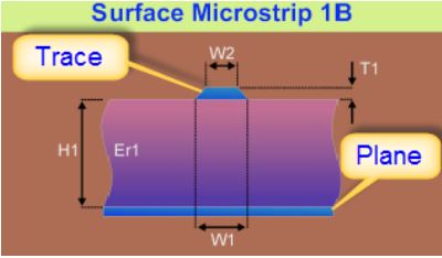
High speed signal transmission in PCB requires the impedances of driver, receiver and that of the PCB transmission lines matched. In case these are not matched, fast logic components in PCBs can produce harmful reflections. To prevent such reflections, it is necessary for the circuit to transmit high-speed signals along paths with a predetermined impedance. The stack-up design helps us to control and define the characteristic impedance of signal traces as per the required target impedance that can minimize reflections and signal distortions. It is obtained by controlling the width of the trace, the thickness of the dielectric material between the trace and its reference plane and the dielectric constant value of the material as shown below:
We can get the desired impedance by using special material for the substrates and controlling their thickness. So meeting controlled impedance tolerances (e.g., ±10%) is important for maintaining signal integrity and preventing reflections. At higher frequencies, via stubs can also cause impedance discontinuities and reflections which severely impacts integrity of the signal. Again a properly designed stack-up can help minimize via stubs and hence their impact.
Crosstalk, Noise, Signal Interference:
When two or multiple signals are running parallel on a PCB for some distance, there is a chance that high-speed signals (aggressor signals) can electromagnetically couple into the other neighboring signal, disturbing the signal quality in the latter signal (victim signal). In general, designers avoid such crosstalk between traces by:
- Increasing the gap between the two traces, if they are on the same layer
- Inserting a ground/power plane between the two traces, if they are on adjacent layers
- Routing the traces so that they are perpendicular to each other
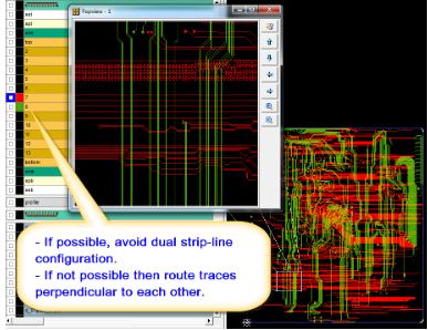
The steps mentioned above are related to the stack-up design. The Er value of the dielectric material used between the two conductor layers drastically impacts the crosstalk between the signals. So a proper stack-up design through the thickness of dielectric layer between signal layers and the use of ground planes, helps minimize capacitive coupling between signal traces, minimizing noise and signal interference.
Signal Timing and Propagation Delays:
In the PCB, the speed of the signals strictly depends upon the value of the effective relative permittivity constant value (Er) of the dielectric material around the signal trace.
v = c / sqrt(Er)
- v = speed of the signal in the medium
- c = speed of light in a vacuum (~3 × 10⁸ m/s)
- εr = relative permittivity (dielectric constant)
So the choice of materials for dielectric and signal layers, ground planes and their order in the PCB stack-up design directly affects signal propagation speeds, delay and signal integrity. In PCBs, the Er value for signals travelling on external layers is lower and hence travel at higher speeds. It is because of the fact that they have air and solder mask layers on one side whose Er values are lower than FR-4 and other substrate dielectric materials.
On the other hand, for signals travelling on inner layers, the effective Er value is higher and hence signals travel at lower speeds on inner layers. So what kind of materials are we using in the stackup, impacts the speed of the signals travelling through them.
EMC Compliance:
A well designed PCB stack-up through proper layer arrangement, dielectric properties and routing strategies, can help achieve excellent EMC compliance. It controls both board’s ability to radiate and be susceptible to electromagnetic interference (EMI). The best strategy is to pair every signal layer with an adjacent GND/PWR plane. It keeps the return current loop areas and their impedances low and hence minimizes the chances of radiation. When required, multiple ground planes can be used for isolation between signals. It also helps PCB designers provide buried capacitance or interplane capacitance by placing power and ground planes very close to each other. Typically, the distance between the two planes is less than 3mil. Further it should be ensured that all critical signals follow a consistent ground reference and avoid crossing voids. PCB level shielding should be used in specific areas to isolate
Stack-up Design – Thermal Concerns:
The manufacturing (fab and assembly) processes and the functionality of the PCB in the fields, expose it to higher temperatures. Since there are different types of materials present in the PCB, all having different values of CTE, these high temperatures can cause different materials to expand at different scales. This phenomenon can put a high force on the PCB and break structures on it causing a malfunction. This can also lead the PCB to warp during the manufacturing processes. Similarly the heat conducting properties of all the materials on the PCB are different from one another. So PCB stack up design directly impacts how the heat is generated and dissipated on the PCB or how the external heat impacts the structures on the PCB. A proper selection of materials for the PCB, their arrangement in the stack-up and following proper design methodologies can ensure reliable PCB operation within acceptable temperature limits through effective heat transfer and temperature control. While selecting materials, we select materials with least disparity in CTE values and choose dielectrics with good thermal conductivity properties to further enhance heat dissipation. Materials with higher thermal conductivity are chosen for the substrate. So choosing metal core substrates can improve heat transfer. In order to conduct the heat from hot areas to cold areas in the PCB or to the external world, we use thermal vias to help keep the temperature low in the PCB. While designing the stack-up, we can control the number of layers, their thickness, and the order in which they are stacked to control heat transfer pathways. In general, thinner the layers and higher the number of layers, more the flexibility for thermal management. We should make sure that all areas in a layer and all layers in the PCB have a balanced amount of Cu in order to avoid uneven thermal stresses in the PCB during the manufacturing processes.
Further, thermal modeling and simulation can help identify potential hotspots, optimize the design for thermal performance and help choose the right materials for the PCB stack-up. This should be done before finalizing the PCB stack-up.
Stack-up Design – Mechanical Integrity:
The stack-up design involves both copper layers and dielectric layers in the form of a multi-layer structure. The configuration of these layers board’s electrical characteristics, mechanical robustness, and thermal properties. The number of layers, their thickness, and the nature of materials selected in the stackup design significantly defines the rigidity and ability of the PCB to withstand stress. That is why we choose different materials for rigid and flex boards. In stack-up designs for flex PCBs, we select light weight and flexible materials to allow for bending and flexibility in movement. The adhesive soldermask materials further add to the mechanical strength of the PCB. We further make sure that the mechanical strength that we ensure through proper number of PCB layers, their thicknesses and the nature of materials is not compromised due to poor design practices like avoiding dropping too many vias close-by to avoid stress concentrations etc. Similarly balancing copper weights helps prevent warpage during the manufacturing process which is very crucial for maintaining mechanical integrity.
So we see how the pathways of the issues related to SI/PI, thermal, mechanical and financial aspects and their solutions stem out of the stackup and terminate into the stackup. The depth of your knowledge and experience of stackup design will define the scope of these aspects as issues or solutions. Rush PCB Inc. always recommends a good stackup design as it will keep your design away from red zones of all of the above high-speed problems.


