

Solder paste printing is the first and most critical step in the Surface Mount Technology (SMT) assembly process. The quality of solder paste deposition directly affects solder joint reliability, component alignment, and overall Printed Circuit Board Assembly (PCBA) yield. Over 60–70% of SMT defects originate from solder paste printing, making it a key focus area for process engineers, particularly for companies like RUSH PCB Inc.
Solder paste consists of finely powdered solder alloy suspended in a flux medium. During printing, solder paste is transferred through a stencil onto PCB pads to form precise deposits that later melt during reflow soldering and create electrical and mechanical connections.
Solder Paste: Definition and Function
Solder paste is a thixotropic material designed to temporarily hold surface-mount components in place and form metallurgical joints during reflow soldering.
Primary functions of solder paste include providing sufficient solder alloy, cleaning pad surfaces through flux action, maintaining deposit shape during placement, and enabling repeatable solder joint formation.
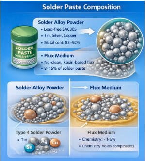
Composition of Solder Paste
Solder Alloy Powder:
The solder alloy typically makes up 85–92% of the paste weight. Common alloys include Sn63/Pb37 and lead-free SAC alloys such as SAC305. Alloy selection depends on regulatory compliance, reliability requirements, and thermal sensitivity.
Flux Medium:
Flux accounts for 8–15% of solder paste and removes oxides, prevents re-oxidation, and promotes wetting. Common flux types include rosin-based, water-soluble, and no-clean fluxes.
Solder Paste Powder Size Classification
Solder powder particle size is classified according to IPC J-STD-005. Smaller particle sizes improve print resolution but increase oxidation risk and cost.
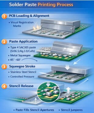
Solder Paste Printing Process Overview
The solder paste printing process is a critical first step in surface mount technology (SMT) assembly, as it determines the volume, shape, and placement accuracy of solder deposits on PCB pads. During this process, solder paste is transferred from the stencil apertures onto the PCB pads using a squeegee system that applies controlled pressure and motion across the stencil surface.
Proper control of printing parameters—such as squeegee speed, pressure, angle, and stencil alignment—ensures uniform paste deposition and accurate pad coverage. Because the quality of solder paste printing directly affects component placement, solder joint formation, and reflow reliability, it is widely regarded as the most influential process step in achieving high-yield and defect-free PCB assembly.
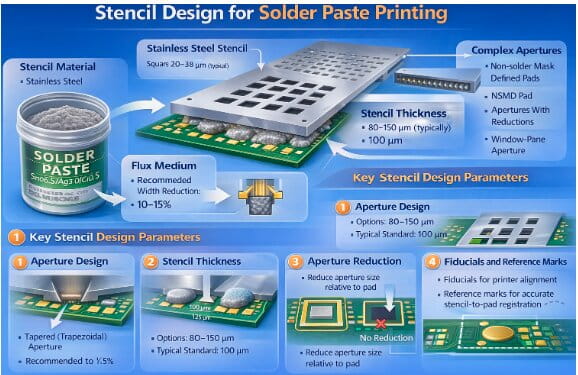
Stencil Design for Solder Paste Printing
Stencil design plays a crucial role in achieving accurate and consistent solder paste deposition during the printing process. A well-designed stencil ensures that the correct volume of solder paste is transferred onto each PCB pad, directly influencing solder joint quality and assembly yield. Key stencil design factors include material selection, stencil thickness, and aperture geometry, all of which must be optimized according to component pitch, pad size, and solder volume requirements.
Stencil Materials
Stencils used for solder paste printing are commonly manufactured from laser-cut stainless steel, which offers good durability, dimensional stability, and cost-effectiveness for standard SMT applications. For fine-pitch and high-density assemblies, electroformed nickel stencils are often preferred due to their smoother aperture walls and more precise feature definition. The improved surface finish of electroformed stencils enhances solder paste release, making them particularly suitable for printing small apertures and ultra-fine-pitch components.
Stencil Thickness
Stencil thickness is a key parameter that determines the volume of solder paste deposited onto PCB pads. Typical stencil thickness values range from 80 to 150 µm, depending on component size, pitch, and solder volume requirements. Thinner stencils are generally used for fine-pitch components to prevent excessive solder deposition and bridging, while thicker stencils are selected for larger components or power devices that require higher solder volumes. Proper selection of stencil thickness ensures balanced solder paste deposition across mixed-technology boards.
Aperture Design
Aperture design has a significant impact on solder paste transfer efficiency and print quality. The shape, size, and reduction of stencil apertures are optimized to improve paste release and minimize printing defects such as bridging and solder balling. Aperture reductions are commonly applied relative to pad dimensions to control solder volume. To ensure reliable paste release, an area ratio of 0.66 or greater is generally recommended, as lower ratios can result in poor paste release and inconsistent deposits. Optimized aperture design is especially critical for fine-pitch and high-density PCB assemblies.
Solder Paste Printing Equipment
Modern SMT production lines employ fully automatic stencil printing machines to achieve high accuracy, repeatability, and throughput in solder paste application. These printers are equipped with advanced vision alignment systems that use fiducial recognition to precisely align the PCB with the stencil before printing, ensuring accurate paste placement even on fine-pitch designs. Controlled squeegee pressure, speed, and angle are applied through programmable motion systems to achieve uniform paste transfer across the stencil apertures. In addition, modern printers offer recipe-based parameter control, allowing printing settings to be optimized and stored for different PCB designs and solder paste types.
The combination of automation, precision control, and real-time monitoring significantly improves print consistency, reduces defects, and enhances overall SMT assembly yield.
Key Printing Process Parameters
The quality and consistency of solder paste deposition depend heavily on precise control of key printing process parameters. Squeegee speed and pressure must be carefully optimized to ensure complete filling of stencil apertures without excessive paste smearing. Stencil separation speed (snap-off) influences paste release and deposit shape, with slower separation generally improving transfer efficiency for fine-pitch designs.
In addition, environmental control, including temperature and humidity, plays an important role in maintaining solder paste viscosity and preventing drying or slumping. Proper control of these parameters ensures uniform solder paste deposits, reduces printing defects, and supports stable SMT production.
Solder Paste Inspection (SPI)
Solder Paste Inspection (SPI) systems are used to evaluate the quality of printed solder paste deposits before component placement. Modern SPI systems measure paste volume, height, area, and positional alignment using 2D or 3D optical inspection techniques. Early detection of printing defects allows corrective action to be taken before reflow, significantly reducing scrap and rework. By providing quantitative data and trend analysis, SPI plays a critical role in improving process stability, yield, and overall PCB assembly quality.
Common Solder Paste Printing Defects
Several types of defects can occur during the solder paste printing process if parameters are not properly controlled.
– Insufficient solder may result from clogged stencil apertures, low squeegee pressure, or dried paste.
– Bridging often occurs due to excessive paste volume, improper aperture design, or misalignment between stencil and PCB.
– Slumping is typically caused by poor paste rheology or high ambient temperature.
– Misalignment can result from inadequate vision alignment or PCB warpage. Understanding the root causes of these defects is essential for effective troubleshooting and process optimization.
Process Control and Best Practices
Effective process control and adherence to best practices are essential for maintaining consistent solder paste printing quality. Regular stencil cleaning prevents paste buildup and aperture clogging, while solder paste life and storage control ensure stable viscosity and performance. Continuous monitoring through SPI trend analysis helps identify process drift before defects occur. In addition, proper operator training and standardized work instructions contribute to consistent setup, operation, and maintenance of printing equipment. Together, these practices improve yield, reduce defects, and enhance process reliability.
Conclusion
Solder paste materials and printing processes form the foundation of reliable PCB assembly, as they directly influence solder joint quality and long-term product performance. Proper selection of solder paste materials, combined with optimized stencil design, precise equipment control, and strict process management, ensures consistent printing results and high production yield. By implementing robust inspection methods and best practices, manufacturers can achieve defect-free assembly and ensure the long-term reliability of electronic products, a standard upheld by RUSH PCB Inc.


