Why You Need an HDI PCB?
As long as electronic products were large, conventional printed circuit boards (PCBs), even complex PCBs, sufficed. However, with the advent of modern smartphones, wearables, and the Internet of Things (IoT), the tendency to go for thinner and smaller products is prevailing. Component manufacturers have responded positively to this trend by making their products ever smaller.
Now, increasingly, everyone wants smaller electronic products with more advanced features. PCBs have also undergone a drastic change in technology, going from thick, rigid structures to thin and flexible types. However, with no relaxation in the trend for reduction in size of products, even thin and flexible PCBs are not enough. Fabricators now use advanced PCB manufacturing techniques to make multilayered boards. These are the High-Density Interconnect (HDI) boards, forming the backbone of the electronic industry.
For instance, mobile phones today are much thinner and lighter than most of their counterparts from just a few years ago. Even so, their functionality is far superior to that of their predecessors. This is because they now use an HDI PCB inside that accommodates far more components and offers substantially improved functionality.
Specifications Leading to Advanced PCB Design
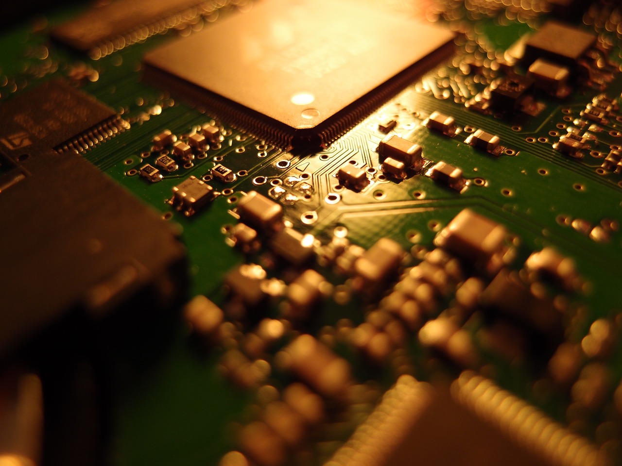
The specifications of modern electronic devices such as wearable electronic devices, requires multi-layer HDI PCB solutions with large number of components on the surface and even within the PCB. This requires fine conductor widths with spaces between them narrower than conventional designs allow. As normal through-hole vias will never fit into the available space, fabricators had to resort to laser-drilled blind and buried microvias.
Manufacturers are making more boards with buried microvias as these help to increase the number of interconnections in the board, while freeing up valuable space on the outer layers for placing more number of components.
Another aspect of such advanced PCB design, apart from microvia technology and increasing number of layers is that complex PCBs are becoming thinner. Fabricators are now using thinner prepregs and cores than they did for conventional designs.
Manufacturing Techniques for Complex PCBs
With use of miniature devices increasing at tremendous speeds, production equipment at PCB factories are under great strain to produce complex PCBs. Producing HDI PCBs requires many of the equipment that conventional board manufacturers also use, as several stages in the fabrication process are similar, however, there are differences. HDI PCB requires working with tiny geometries that only sophisticated equipment can handle.
For instance, complex PCBs made with HDI technology incorporate blind and or buried microvias in the several layers that make up the stack. Making these microvias not only requires several additional steps, but the fabricator has to repeat these steps several times. The repetition increases the complexity and the risk of error.
Also Read: Different Stackups for HDI PCBs
Drilling the microvias needs laser drills, and making good quality, reliable HDI PCBs requires appropriate plating equipment and professionals with processing experience. For instance, most microvias will have holes of diameter 50 µm on average, and the latest machines can drill hundreds of such holes per second.
Conventional image transfer techniques do not work for HDI boards, as they are unable to handle the 50 µm features common for these complex PCBs. Fabricators have to use laser direct imaging systems for transferring the pattern directly on the photo-imageable material bonded onto the surface of each layer.
As features of these advanced PCBs are very small, the transfer of images requires very clean rooms to prevent contamination from airborne particles and human hair. It also requires the rooms to have good control over humidity levels and temperature.
The tiny microvias of HDI PCBs need a different treatment for plating them as compared to the more conventional plating techniques. Mechanical and air bubble agitation suitable for ordinary plating lines do not work for HDI boards as the plating chemicals do not flow well through the 100 µm and lower diameter holes. Fabricators must use both vertical continuous plating lines and horizontal plating lines for ensuring proper plating of microvias by spraying the plating chemicals into the pads under high pressure.
The smaller features of the HDI PCBs make it more difficult to position the coverlay or solder mask properly against the pattern. Rather than using the conventional screening methods, fabricators prefer to use special laser direct imaging techniques to deposit the solder mask. This requires development of new types of solder mask inks.
Advantages of Using HDI PCBs
Although the traditional market for such advanced PCBs designed and fabricated with the HDI technology has been the smart phones and mobile phones, nearly all intelligent equipment use HDI for their boards.
The main advantage with the HDI technique is the possibility of populating PCBs with denser BGA and QFP packages. The development of high-speed serial bus technology is pushing the signal transmission rates upwards continuously. HDI technology, with its smaller features offers reduction of several parameters to ensure higher wiring density, better electrical performance and improved signal integrity. This is especially helpful in medical equipment and other emerging product areas such as car electronics and communication base stations.
The use of thinner substrate material for prepreg in HDI technology has the advantage of improving the heat transfer across the boards. Moreover, the fabricator can select the material to have high electrical resistance but lower thermal resistance. Therefore, heat removal is more efficient from the densely packed PCBs and all components on the PCB operate within their safety zones.
At very high frequencies, the dielectric loss becomes the predominant loss mechanism, with heat energy lost as the substrate charges and discharges. However, fabricators of HDI PCBs have access to a vast range of base materials that offer very low loss to ultra-low losses. Although the designer cannot avoid dielectric losses altogether, the use of low-loss materials for HDI PCBs allows the dielectric losses to become the main loss mechanism only at much higher frequencies than it normal happens.
Conclusion
With ever-increasing speeds of signals on the PCB, and the prolific use of miniature components driven by the shrinking size of electronic devices, designers and fabricators find the use of HDI techniques very helpful in fabricating advanced PCBs for achieving better features, quality, and reliability.